July 2015

Graphene-based flat pack batteries offer improved performance

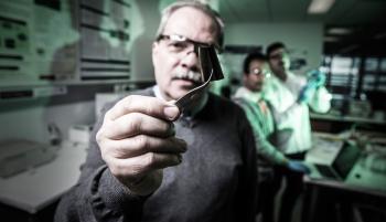
Researchers at the University of Wollongong's Institute for Superconducting and Electronic Materials designed a graphene-based flexible, foldable, and lightweight energy storage device for use in next-gen wearable technology and also as a potential device for medical implants, like pacemakers.
The scientists devised a 3D structure:  liquid graphene was mixed with a polymer and the combination was then solidified to form the carbon nanotubes. The resulting structure was made-up of three parts: graphene, a conductive polymer, and carbon nanotubes. These three parts take the form of single atom-thick networks, resembling carbon formed cylinders. The novel design is efficient because by separating out the layers of carbon, researchers are able to use both surfaces in the structure for charge accumulation. The scientists expect this design to lead to ultra-fast and efficient battery devices. 

Read the full story Posted: Jul 30,2015

Graphene to enable color-tunable LEDs

Researchers from Tsinghua University in Beijing demonstrated a graphene-based LED that not only can be tuned to emit different colors of light, but can do so across nearly the entire visible spectrum: from blue (450-nm wavelength) to red (750-nm wavelength)—basically all colors but the darkest blues and violets. Such a color tunable LED has never before been realized.

The scientists made the light-emitting material from the interface of two different forms of graphene. These forms are graphene oxide (GO) and reduced graphene oxide (rGO). Placed at the interface of the GO and rGO is a special type of partially reduced GO that has optical, physical, and chemical properties that lie somewhere in between those of GO and rGO. The most important "blended" property of the interfacial layer is that it has a series of discrete energy levels, which ultimately allows for the emission of light at many different energies, or colors.

Read the full story Posted: Jul 29,2015

Angstron Materials secures $5 million to expand business and commercialize key products

The U.S-based graphene materials producer and applications developer Angstron Materials announced securing $5 million in capital to increase manufacturing capacity for its single and few-layer graphene materials and bring key technologies to market.

The company began seeking Pre-Series A funding in late 2014. According to the company, the investment partner (only named as a "key player in advanced materials and consumer electronics") brings extensive business and industry expertise to the table, along with a portfolio of major customers and collaborators.

Read the full story Posted: Jul 29,2015

Monash and Ionic cooperate to design graphene-based supercapacitors

Ionic Industries, a spin-off of minerals explorer Strategic Energy Resources, cooperated with Monash University to develop extremely thin graphene-based supercapacitors, able to store large amounts of energy. According to Ionic, the first battery prototype should be available within six months and more sophisticated prototypes in three to five years.

The supercapacitors are tiny - smaller than the diameter of human hair, actually. They were created following two years of rigorous experiments, using an ion beam to etch the supercapacitors on to wafers made of graphene. They are said to be able to be fully recharged in minutes and last longer than present battery technologies.

Read the full story Posted: Jul 28,2015

Apple patents Lightning connectors with graphene signal paths

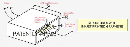
Apple recently submitted a patent application for lightning connectors that use graphene signal paths. In Apple's patent a connector (lightning connector) is coupled to a signal cable. The inkjet-printed graphene traces are formed on the upper and/or lower surfaces of the plastic connector tongue.

A connector can be provided with dielectric material and conductive traces, some of which can be made using printed circuits. Graphene traces may be deposited using inkjet printing techniques or other deposition and patterning techniques. During inkjet printing, graphene may be patterned to form signal lines on a connector structure, printed circuit, contacts on a printed circuit board and other structures. 

Read the full story Posted: Jul 27,2015

Graphene Lighting PLC to start trading in the Canadian stock exchange

Graphene Lighting PLC has signed a letter of intent to engage in a reverse takeover with Canadian capital pool company Oriana Resources Corp. Gaining a stock exchange listing in Canada is in line with Graphene Lighting’s intention to become a global supplier of graphene-enabled light bulbs and lighting systems. 

Oriana and Graphene Lighting will complete the reverse takeover by way of a share exchange arrangement that will make Graphene Lighting a wholly-owned subsidiary of Oriana. The completion of the deal is subject to a number of conditions, like the closing of a $5 million brokered private placement of subscription receipts by Graphene Lighting, and using the proceeds to execute Graphene Lighting’s product development, sales and marketing strategy.

Read the full story Posted: Jul 27,2015

Israeli and Australian scientists come up with a fast and efficient method of producing graphene

Researchers at the Israeli Ben-Gurion University of the Negev (BGU) and University of Western Australia have designed a new process for creating few-layer graphene for use in energy storage and other material applications that is faster, potentially scalable and surmounts some of the current graphene production limitations.

The new one-step, high-yield generation process is based on an ultra-bright lamp-ablation method and has succeeded in synthesizing few-layer (4-5) graphene in relatively high yields. It involves a novel optical system (originally invented by BGU professors) that reconstitutes the immense brightness within the plasma of high-power xenon discharge lamps at a remote reactor, where a transparent tube filled with simple, inexpensive graphite is irradiated. The process is considered fast, safe and green (free of any toxic substances - just graphite plus concentrated light).

Read the full story Posted: Jul 25,2015

Graphene-enhanced composite to convert engine heat into electrical energy

Scientists from the UK, including ones from Manchester University, used graphene to develop a material that could convert an engine heat into electrical energy to help keep a car running (instead of going to waste) and reduce the need for fuels. It could also have applications in aerospace, manufacturing and other sectors.

Compounds that are able to capture waste heat from engines and other power systems and turn it into electricity are usually heavy, costly, toxic or only operate at high temperatures. The scientists in this study took a material called strontium titanium dioxide and added a small amount of graphene. The resulting composite was able to capture and convert heat into electric current efficiently over a broad temperature range.

Read the full story Posted: Jul 24,2015

Valence Industries to start selling graphene within the next year

Valence Industries logoValence Industries, the Australian graphite producer, confirmed it would start selling graphene in the next 6 to 12 months. No definite details were given as to the kind of graphene or the place of production, but it is reasonable to assume that this move stems from Valence's cooperation with Adelaide University to establish a graphene research center in South Australia, announced in March 2014.

Read the full story Posted: Jul 23,2015

Scientists utilize ion implantation methods to create graphene on silicon

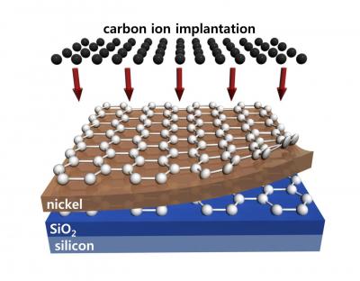
Researchers from Korea University have developed a simple and microelectronics-compatible method to grow graphene and have declared the successful synthesis of wafer-scale (four inches in diameter), high-quality, multi-layer graphene on silicon substrates. The method is based on an ion implantation technique, a process in which ions are accelerated under an electrical field and smashed into a semiconductor. The impacting ions change the physical, chemical or electrical properties of the semiconductor.

Ion implantation is a technique normally used to introduce impurities into semiconductors. In the process, carbon ions were accelerated under an electrical field and bombarded onto a layered surface made of nickel, silicon dioxide and silicon at the temperature of 500 degrees Celsius. The nickel layer, with high carbon solubility, is used as a catalyst for graphene synthesis. The process is then followed by high temperature activation annealing (about 600 to 900 degrees Celsius) to form a honeycomb lattice of carbon atoms, a typical microscopic structure of graphene.

Read the full story Posted: Jul 22,2015