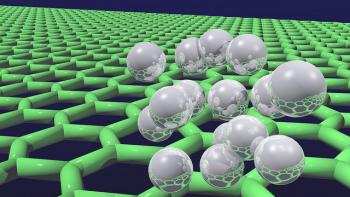
Researchers at the University of Illinois designed a single-step method of creating textures in graphene ("crumpling") to allow for larger surface areas, thus tapping into graphene's benefits for electronics. The scientists believe that "crumpled" graphene may also be used as high surface area electrodes for batteries and supercapacitors. As a coating layer, the 3D graphene could allow omniphobic/anti-bacterial surfaces for advanced coating applications.

The "crumpling" process is based on a known shape-memory polymer substrate (a material capable of returning to its original shape after being distorted, mostly by thermal means). The thermoplastic nature of the substrate also allows for the crumpled graphene morphology to be arbitrarily re-flattened at the same elevated temperature for the crumpling process.
In October 2014, MIT researchers discovered that "crumpling" graphene may enable foldable and stretchable energy devices.