Researchers at North Carolina State University have developed a technique that enables the integration of graphene, graphene oxide (GO) and reduced graphene oxide (rGO) onto silicon substrates at room temperature by using nanosecond pulsed laser annealing. The advance may open the door to the possibility of creating new electronic devices, such as smart biomedical sensors.
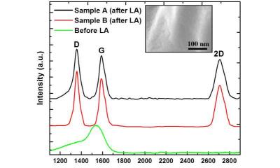
In this new technique, the researchers start with a silicon substrate. They top that with a layer of single-crystal titanium nitride, using domain matching epitaxy to ensure the crystalline structure of the titanium nitride is aligned with the structure of the silicon. They then place a layer of copper-carbon alloy on top of the titanium nitride, again using domain matching epitaxy. Finally, the researchers melt the surface of the alloy with nanosecond laser pulses, which pulls carbon to the surface.
The team states that this process can easily be scaled up; so far they have made wafers that are two inches square, and could reportedly make them much larger, using lasers with higher Hertz at room temperature, which drives down the cost.
"We have already patented the technique and are planning to use it to develop smart biomedical sensors integrated with computer chips,"the researchers say.