IBM researchers developed a new process that can be used to fabricate single-oriented, single-layer graphene at wafer-scale. The process uses two exfoliation stages, and the researchers managed to made graphene wafers 4" in size. The researchers believe that in the future graphene will replace silicon as a transistor technology (they quote Nature's estimate of 2021) - and graphene based transistors will achieve speeds of 1 Thz over the next decade.
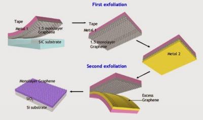
This process uses the idea that every element in the periodic table has a different adhesion (atomic binding energy) to graphene. They start by growing graphene on a silicon carbide (SiC) substrate, and then separate the graphene from the SiC by using a stressed nickel layer. Then they perform a second exfoliation that removes any graphene in excess of a single-layer by using a thin gold layer thus leaving only single-layer, single-oriented graphene.
One of the advantages of this technique that the SiC wafer is reusable - which lowers the production cost.
Source: IBM