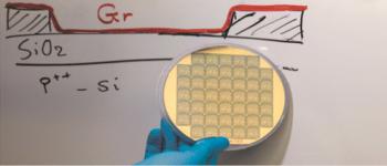
Scientists from Germany, the Netherlands, Spain and Saudi Arabia, along with Graphenea, designed an improved process for achieving wafer-scale fabrication of graphene devices. The process is said to be reliable and produce graphene sheets that are smooth and uniform across the wafer, conformally covering the electrode structures.

The process relies on a series of actions that overturns traditional fabrication norms - lithography and contact evaporation are performed prior to graphene transfer. In the research, the scientists studied the values reported in literature for contact and sheet resistance obtained with the standard graphene fabrication and transfer method. Focusing on graphene grown by CVD, they found that there is significant scatter in the reported values. The scientists then performed the standard procedure themselves, finding that the resulting graphene sheet is inhomogeneous, with defects appearing in random places.
The improved process, in which the contact patterning and metal deposition are performed prior to the transfer, yields a much better result. Electrical measurements indicate good device reproducibility, with sheet resistance low enough to consider using these graphene devices in radio frequency electronics. The potential application of the graphene channels is additionally confirmed by steady device performance over a wide range of applied current, up to 0.5 A. The careful fabrication led to devices that support the highest current density ever reported in transferred CVD graphene.