Researchers from the Beckman Institute have researchers the electronics behavior of graphene with grain boundaries. They explain that when graphene is grown, lattices of the carbon grains are formed randomly, linked together at different angles of orientation in a hexagonal network. But sometimes when the process is not perfect, defects called grain boundaries (GBs) form. These boundaries scatter the flow of electrons in graphene, which harms the material's electronic performance.
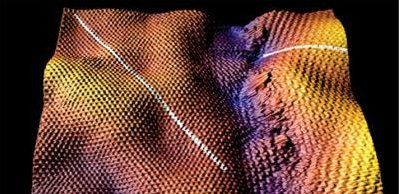
The researchers grew polycrystalline graphene on a silicon wafer using CVD, and then examined the atomic-scale grain boundaries using scanning tunneling microscopy and spectroscopy. The electron scattering at the boundaries significantly limits the electronic performance compared to grain boundary free graphene. In fact they say that when the electrons' itinerary takes them to a grain boundary, it is like hitting a hill - the electrons bounce off, interfere with themselves and create a wave pattern. The hill slows the electrons down - which means that the grain boundary is a resistor in series with a conductor.