Researchers from the US, Germany, Singapore and Spain developed a new way to image and study grain boundary defects in graphene using surface plasmons. The idea is that by analyzing how the surface plasmons are reflected and scattered you can understand more about those defects. The researchers discovered that grain boundaries act as electronic barriers around 1020 nm in size and they are responsible for the CVD-grown graphene's low electron mobility.
In addition, the researchers say that the grain boundaries may actually be useful in the future - perhaps used as tuneable plasmons reflectors and phase retarders in "plasmonic circuits".
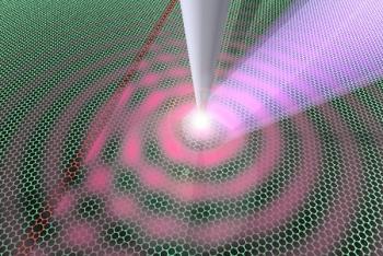
While defect-free graphene has excellent mechanical and electrical properties, in practice large CVD-grown graphene sheets aren't so good. This is because those sheets are actually made from smaller graphene sheets "patched together", and the boundaries are defects that cause the graphene to be weaker and less conductive. The researchers developed a new imaging technique that analyses surface plasmon waves (coherent oscillations of electrons) induced on the graphene surface when the material is "perturbed" by a nanoscale antenna (an atomic force microscope tip, seen in the image above) excited by infrared light. The plasmon waves are reflected and scattered by the graphene grain boundaries, so creating plasmon interference.
This is the last of many researches into graphene's grain boundaries. In January 2013 researchers from the Beckman Institute already demonstrated how those boundaries effect the electronic properties of graphene.