Canada-based University of Guelph to receive grant for graphene research

A professor at the University of Guelph in Canada is receiving $1.4 million CAD (a little over $1 million USD) over the next seven years toward his research, which includes developing practical graphene applications. Prof. Aichen Chen was recently named as a tier-1 Canada Research Chair in electrochemistry and nanoscience, a title that came with the $1.4 million in funding.

For the past five years, Chen has been working with graphene — aiming to use it to create innovative green technologies for projects like energy storage and clean drinking water.
Read the full story Posted: Nov 19,2018

Researchers manipulate the width of GNRs to create quantum chains that could be used for nano-transistors and quantum computing

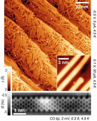
Researchers at EMPA (Swiss Federal Laboratories for Materials Science and Technology), along with colleagues from the Max Planck Institute for Polymer Research in Mainz and other partners, have succeeded in precisely controlling the properties of graphene nano-ribbons (GNRs) by specifically varying their shape. This can be used to generate specific local quantum states, and could in the future be used for precise nano-transistors or possibly even quantum computing.

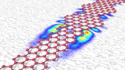
Researchers manipulate the width of GNRs to create quantum chains that could be used for nano-transistors and quantum computing image

The team has shown that if the width of a narrow graphene nano-ribbon changes, in this case from seven to nine atoms, a special zone is created at the transition: because the electronic properties of the two areas differ in a special, topological way, a "protected" and thus very robust new quantum state is created in the transition zone. This local electronic quantum state can be used as a basic component to produce tailor-made semiconductors, metals or insulators - and perhaps even as a component in quantum computers.

Read the full story Posted: Aug 12,2018

Puzzling results explained: a multiband approach to Coulomb drag and indirect excitons in dual-layer graphene

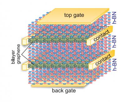
A theoretical collaborative study by the University of Antwerp (Belgium), the University of Camerino (Italy) and the University of New South Wales (Australia) has explained previously mystifying experimental results obtained independently by two research groups in the USA, which showed coupled holes and electrons in dual-layer graphene structures sometimes moved in exactly the opposite direction to that predicted.

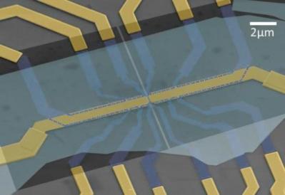
A multiband approach to Coulomb drag and indirect excitons in dual-layer graphene imageDevice schematic: one sheet of conductive bilayer graphene carries electrons, the other, separated by insulating hBN, carries holes

The new work showed that this apparently contradictory phenomenon is associated with the bandgap in dual-layer graphene structures, a bandgap which is very much smaller than in conventional semiconductors.

Read the full story Posted: Jul 19,2018

International team produces nano-transistors from carefully controlled GNRs

An international team of researchers from Empa, the Max Planck Institute for Polymer Research in Mainz and the University of California at Berkeley has succeeded in growing graphene ribbons exactly nine atoms wide with a regular armchair edge from precursor molecules. The specially prepared molecules are evaporated in an ultra-high vacuum for this purpose. After several process steps, they are put on a gold base to form the desired nanoribbons of about one nanometer in width and up to 50 nanometers in length.

Researchers create GNR-based transistors image

These structures have a relatively large and, most importantly, precisely defined energy gap. This enabled the researchers to go one step further and integrate the graphene ribbons into nanotransistors. Initially, however, the first attempts were not so successful: Measurements showed that the difference in the current flow between the "ON" state (i.e. with applied voltage) and the "OFF" state (without applied voltage) was far too small. The problem was the dielectric layer of silicon oxide, which connects the semiconducting layers to the electrical switch contact. In order to have the desired properties, it needed to be 50 nanometers thick, which in turn influenced the behavior of the electrons.

Read the full story Posted: Dec 01,2017

A new method to control electrons in graphene may open the door to next-gen electronics

Scientists at Rutgers University-New Brunswick have found a way to control the electrons in graphene, paving the way for the ultra-fast transport of electrons with low loss of energy in novel systems. "This shows we can electrically control the electrons in graphene," said a professor in Rutgers' Department of Physics and Astronomy. "In the past, we couldn't do it. This is the reason people thought that one could not make devices like transistors that require switching with graphene, because their electrons run wild."

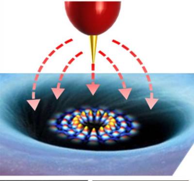
Controlling electrons in graphene image

This new work might make it possible to realize a graphene nano-scale transistor, the team said, which would be an important step towards an all-graphene electronics platform. The team managed to control electrons by sending voltage through a microscope with an extremely sharp tip, also the size of one atom, which offers 3-D views of surfaces at the atomic scale. The microscope's sharp tip creates a force field that traps electrons in graphene or modifies their trajectories, similar to the effect a lens has on light rays. Electrons can easily be trapped and released, providing an efficient on-off switching mechanism, according to the team.

Read the full story Posted: Oct 23,2017

Graphene nano-ribbons give a major boost to the sensitivity of sensors

Researchers from the University of Nebraska-Lincoln, University of Illinois at Urbana-Champaign, and Russia’s Saratov State Technical University have shown that adding a graphene nanoribbons to gas sensors can significantly increase their sensitivity compared to traditional ones.

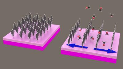
GNRs improve efficiency of gas sensor imageThis rendering shows gas molecules widening the gaps between rows of the team's GNRs. This was proposed as a partial explanation to how the nano-ribbons grant sensors an unprecedented boost

The team integrated the nano-ribbons into the circuity of the gas sensor where it reportedly responded about 100 times more sensitively to molecules than did sensors featuring even the best performing carbon-based materials. With multiple sensors on a chip, we were able to demonstrate that we can differentiate between molecules that have nearly the same chemical nature, said the study author and associate professor of chemistry at the University of Nebraska. For example, we can tell methanol and ethanol apart. So these sensors based on graphene nano-ribbons can be not only sensitive but also selective.

Read the full story Posted: Oct 22,2017

MIT and Johns Hopkins team manages to make graphene self-fold into 3D shapes

Researchers with Johns Hopkins University and MIT have shown a way to cause flat sheets of graphene to self-fold into 3D geometric shapes. The group explains how they prepared the sheets and then used heat to cause them to fold. The ability to create 3D objects from sheets of graphene can advance opportunities in fields like sensors, wearables and more.

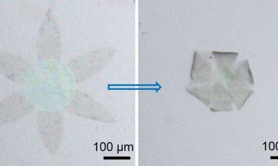
Graphene can be folded into 3D shapes image

In their work, the researchers developed a micro-patterning technique that leads to the flat graphene sheets bending along predesignated lines when heat is applied, causing the sheet to form into shapes. The new method not only preserves the intrinsic properties of the graphene, but it was also found that the creases can cause a band gap in the graphene, which can be extremely useful.

Read the full story Posted: Oct 10,2017

Researchers manipulate graphene to bring it closer to transistor applications

Researchers at the U.S. Department of Energy’s Ames Laboratory successfully manipulated the electronic structure of graphene, which may enable the fabrication of graphene transistors that could be faster and more reliable than existing silicon-based transistors.

Ames Lab manipulates graphene image

The researchers were able to theoretically calculate the mechanism by which graphene’s electronic band structure could be modified with metal atoms. The work will guide experimentally the use of the effect in layers of graphene with rare-earth metal ions sandwiched (intercalated) between graphene and its silicon carbide substrate. Since the metal atoms are magnetic, the additions can also modify the use of graphene for spintronics.

Read the full story Posted: Aug 30,2017

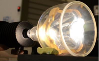
Researchers develop an efficient and healthy laser-induced graphene foam lighting device

Researchers from the Institute of low temperature and structure research in Wroclaw, Poland, developed a new efficient white light source that uses graphene foam excitated by a continuous-wave laser. The laser opens up a bandgap in graphene which results in light emission that ranges from 360nm (UV) or 405nm (visible) to 980nm-1064nm (near-infrared).

Graphene foam based white-light source (wroclaw)

The researchers say that the light spectrum of this device is similar to the spectrum of the sun which is better than current light sources such as LEDs that offer light spectrum with strong peaks (the main problem is the strong blue light emission in LED lighting). This design can achieve a high efficiency (over 200 lm/W), high color rendering index (CRI > 99) and a broadband warm white color. The lifetime depends on the laser, which can be over 10,000 hours.

Read the full story Posted: May 19,2017

Valleytronics research advances thanks to bi-layer graphene

Researchers from Penn State University demonstrated a new device, based on bi-layer graphene, that provides an experimental proof of the ability to control electron-flow by the valley degree of freedom. Valleytronics is a new field of science that aims to create devices that use electron's valley degree of freedom (in a somewhat similar way to Spintronics that aims to do the same with electron spin).

Bi-layer graphene based valleytronics experiment (Penn State)

The device is built from bi-layer graphene. The researchers added an electric field perpendicular to the plane opens a bandgap in the bi-layer graphene, which then enables them to build valleytronics valves in a physical gap present in the device.

Read the full story Posted: Aug 31,2016