Boron Nitride

Researchers observe fractional quantum anomalous Hall effect in multilayer graphene

Researchers at MIT and Japan's National Institute for Materials Science (NIMS) have observed an exotic electronic state in a material made of five layers of graphene, that could enable new forms of quantum computing. 

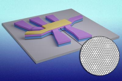
Generally speaking, the electron is the basic unit of electricity, as it carries a single negative charge. At least, that's the case in most materials in nature. But in very special states of matter, electrons can splinter into fractions of their whole. This phenomenon, known as “fractional charge,” is extremely rare, and if it can be corralled and controlled, the exotic electronic state could help to build resilient, fault-tolerant quantum computers. To date, this effect, known to physicists as the “fractional quantum Hall effect,” has been observed a handful of times, and mostly under very high, carefully maintained magnetic fields. Now, the scientists have also seen the effect in a material that did not require such powerful magnetic manipulation. They found that when five sheets of graphene are stacked like steps on a staircase, the resulting structure inherently provides just the right conditions for electrons to pass through as fractions of their total charge, with no need for any external magnetic field.
Read the full story Posted: Feb 22,2024

Rice researchers map the diffusion of graphene and hexagonal boron nitride in aqueous solutions

Rice University researchers have mapped out how bits of 2D materials move in liquid ⎯ which that could help scientists assemble macroscopic-scale materials with the same useful properties as their 2D counterparts.

In order to maintain these special properties in bulk form, sheets of 2D materials have to be properly aligned ⎯ a process that often occurs in solution phase. The Rice team focused on graphene and hexagonal boron nitride, a material with a similar structure to graphene but composed of boron and nitrogen atoms.

Read the full story Posted: Feb 04,2024

Researchers design graphene biosensor that uses sound waves for chemical fingerprinting of ultrathin biolayers

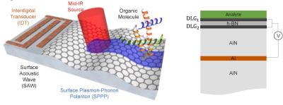
Universidad Politécnica de Madrid researchers have reported the development of an electrically tunable graphene-based biosensor that leverages sound waves to provide unprecedented infrared sensitivity and specificity at the single layer limit. By precisely matching the tunable graphene plasmon frequency to target molecular vibrations, even faint spectral fingerprints emerge clearly.


This acoustically activated approach enables precise in situ study of angstrom-scale films, unlocking new infrared applications across chemistry, biology and medicine.

Read the full story Posted: Jan 23,2024

Researchers use graphene and boron nitride to develop new brain-like transistor that mimics human intelligence

Researchers at Northwestern University, MIT, Harvard University, CIFAR Azrieli Global Scholars Program and Japan's National Institute for Materials Science have developed a graphene-based synaptic transistor capable of higher-level thinking.

The device simultaneously processes and stores information just like the human brain. In new experiments, the researchers demonstrated that the transistor goes beyond simple machine-learning tasks to categorize data and is capable of performing associative learning.

Read the full story Posted: Dec 25,2023

Researchers develop 'golden rules' for controlling alignment of supermoiré lattices

Researchers from Singapore's National University of Singapore (NUS) and Japan's National Institute for Materials Science (NIMS) have formulated 'golden rules' for controlling the alignment of supermoiré lattices. 

Moiré patterns are formed when two identical periodic structures are overlaid with a relative twist angle between them or two different periodic structures but overlaid with or without twist angle. The twist angle is the angle between the crystallographic orientations of the two structures. For example, when graphene and hexagonal boron nitride (hBN) which are layered materials are overlaid on each other, the atoms in the two structures do not line up perfectly, creating a pattern of interference fringes, called a moiré pattern. This results in an electronic reconstruction. The moiré pattern in graphene and hBN has been used to create new structures with exotic properties, such as topological currents and Hofstadter butterfly states. When two moiré patterns are stacked together, a new structure called supermoiré lattice is created. Compared with the traditional single moiré materials, this supermoiré lattice expands the range of tunable material properties allowing for potential use in a much larger variety of applications.

Read the full story Posted: Sep 04,2023

Researchers study ‘sandwich’ of graphene and boron nitride for next-gen microelectronics

Graphene conducts electricity well – too well, in fact, to be useful in microelectronic technology. But by sandwiching graphene between two layers of boron nitride, which also has a hexagonal pattern, a moiré pattern results. The presence of this pattern is accompanied by dramatic changes in the properties of the graphene, essentially turning what would normally be a conducting material into one with (semiconductor-like) properties that are more amenable to use in advanced microelectronics. But in order to harness this potential for industrial use, there is first a need to better understand the dynamics. 

Researchers from University at Buffalo, Japan's National Institute for Materials Science and Chiba University, Chinese Academy of Sciences (CAS), Thailand's King Mongkut’s Institute of Technology Ladkrabang and Korea's Sungkyunkwan University have chosen a strategy of rapid electrical pulsing to drive carriers in graphene/hexagonal boron nitride (h-BN) heterostructures deep into the dissipative limit of strong electron-phonon coupling. By using electrical gating to move the chemical potential through the “Moiré bands”, they show a cyclical evolution between metallic and semiconducting states. The team's results demonstrate how a treatment of the dynamics of both hot carriers and hot phonons is essential to understanding the properties of functional graphene superlattices. 

Read the full story Posted: Apr 21,2023

Researchers use graphene to design transformable nano-scale electronic devices

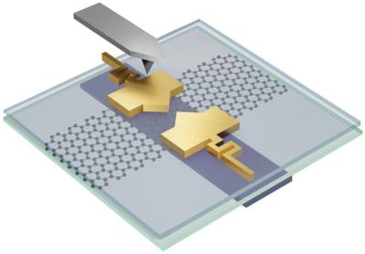
Researchers at University of California, Irvine, working with a team from Japan's National Institute for Materials Science, have reported the discovery of nano-scale devices that can transform into many different shapes and sizes even though they exist in solid states. This comes in contrast to conventional nano-scale electronic parts in devices like smartphones, that are solid, static objects that once designed and built cannot transform into anything else. This recent finding could fundamentally change the nature of electronic devices, as well as the way scientists research atomic-scale quantum materials. 

 Schematic of an hBN-encapsulated graphene device with a local graphite back gate and flexible serpentine leads connected to the movable QPC top gates (metal contacts to the graphene and graphite not shown). Image from Science Advances

“What we discovered is that for a particular set of materials, you can make nano-scale electronic devices that aren’t stuck together,” said Javier Sanchez-Yamagishi, an assistant professor of physics & astronomy whose lab performed the new research. “The parts can move, and so that allows us to modify the size and shape of a device after it’s been made.”

Read the full story Posted: Apr 19,2023

Graphene quantum dots could improve magnetic field sensors

Researchers from the University of California Santa Cruz, University of Manchester and Japan's International Center for Materials Nanoarchitectonics and National Institute for Materials Science have used a scanning tunnelling microscope to create and probe single and coupled electrostatically defined graphene quantum dots, to investigate the magnetic-field responses of artificial relativistic nanostructures.

Trapped electrons traveling in circular loops at extreme speeds inside graphene quantum dots are highly sensitive to external magnetic fields and could be used as novel magnetic field sensors with unique capabilities. Although graphene electrons do not move at the speed of light, they exhibit the same energy-momentum relationship as photons and can be described as "ultra-relativistic." When these electrons are confined in a quantum dot, they travel at high velocity in circular loops around the edge of the dot.

Read the full story Posted: Mar 07,2023

Graphene used to grow the world's smallest microLEDs and highest-density microLED arrays

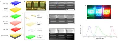
Researchers from MIT, in collaboration with researchers from other Universities in the US and Korea, have used graphene (and hBN) to develop full-color vertically-stacked microLEDs  - that achieve the highest array density (5100 PPI) and the smallest size (4 µm) reported to date.

The researchers developed a 2D-materials based layer transfer (2DLT) technique - that involves growing the LEDs on 2D material-coated substrates, removing the LEDs, and then sttacking them. For the red LEDs, the researchers used graphene, coated on a GaAs wafer, while for the green and blue LEDs, they used hBN on sapphire wafers. The graphene red LEDs were transferred using remote epitaxy, while the hBN blue and green ones were removed using Van der Waals epitaxy.

Read the full story Posted: Feb 02,2023

Researchers find superconductivity that can be turned on and off in "magic angle" graphene

Researchers at MIT and National Institute for Materials Science in Tsukuba, Japan, have found a new and intriguing property of “magic-angle” graphene: superconductivity that can be turned on and off with an electric pulse, much like a light switch.

The discovery could lead to ultrafast, energy-efficient superconducting transistors for neuromorphic devices — electronics designed to operate in a way similar to the rapid on/off firing of neurons in the human brain.

Read the full story Posted: Jan 29,2023