Researchers at the University of Wisconsin-Madison have discovered a way of growing graphene nanoribbons with desirable semiconducting properties directly on a conventional germanium semiconductor wafer. This finding may allow manufacturers to easily use graphene nanoribbons in hybrid integrated circuits, which promise to deliver a major boost to the performance of next-gen electronic devices. This technology could also have specific uses in industrial and military applications, such as sensors that detect specific chemical and biological species and photonic devices that manipulate light.
The technique for producing graphene nanoribbons is said to be scalable and compatible with the prevailing infrastructure used in semiconductor processing - nanoribbons that can be grown directly on the surface of a semiconductor like germanium are more compatible with planar processing used in the semiconductor industry, and so would pose less of a barrier to integrating these materials into electronics in the future.
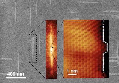
To be put to optimal use, graphene nanoribbons need to be less than 10 nanometers wide. In addition, the nanoribbons must have smooth, well-defined armchair edges in which the carbon-carbon bonds are parallel to the length of the ribbon. top-down fabrication approaches in which lithographic techniques are used in order to cut larger sheets of graphene into ribbons lack precision and produce nanoribbons with rough edges, while "bottom-up" techniques only work on metal substrates.
The innovative technique in this study is a bottom-up technique in which ultra-narrow nanoribbons with smooth, straight edges are grown directly on germanium wafers using CVD. The researchers start with methane, which adsorbs to the germanium surface and decomposes to form various hydrocarbons. These hydrocarbons react with each other on the surface, where they form graphene.
The team made its breakthrough when it explored dramatically slowing the growth rate of the graphene crystals by decreasing the amount of methane in the CVD chamber. They found that at a very slow growth rate, the graphene crystals naturally grow into long nanoribbons on a specific crystal facet of germanium. By simply controlling the growth rate and growth time, the researchers can easily tune the nanoribbon width be to less than 10 nanometers.
The nanoribbons produced using this method start growing at seemingly random spots on the germanium and are oriented in two different directions on the surface. The team’s future work will include controlling where the ribbons start growing and aligning them all in the same direction.