November 2012

New graphene-based device could lead to spintronic switches

Researchers from Germany, Russia and the USA managed to increase graphene's conduction electrons' spin-orbit coupling by a factor of 10,000. They say this could enable a Spintronics switch that is controlled by a small electric field. To develop this, the researchers placed graphene on a nickel substrate in which atoms are separated by the same distance as the graphene's hexagonal meshes. They then deposited gold atoms on the device which ended up between the graphene and nickel sheets.
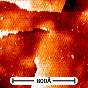
The electrons in the graphene layer exhibited an increased spin-orbit coupling - in fact 10,000 stronger compared to a regular graphene sheet. They say that such a strong spin-orbit coupling could be used to develop a Spintronics switch - in which the spin can be rotated using an electric field. The switch will include two perpendicular spin filters that will be controlled by the electric field.
Read the full story Posted: Nov 29,2012

New method to make ordered GO with good electronic properties

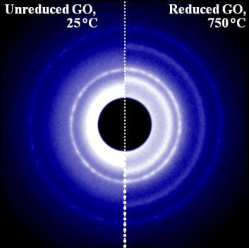
Unlike graphene, graphene-oxide (GO) has a bandgap, but has poor electronic properties (due to disorganized arrangement of atoms). Now researchers from the University of Wisconsin—Milwaukee have developed a method to make ordered GO. They hope that this method will enable "ideal bandgap" carbon based devices to be used as transistors, sensors and optoelectronic devices.

The researchers made a device made from layers of oxygen-poor graphene sandwiched between layers of GO, and then annealed (heated) it. The resulting device (shown on the right of the image above) has a more complex and ordered structure (you can see this as the extra rings in the image).

Read the full story Posted: Nov 28,2012

AZ Electronic Materials license Rice University's GNR technology, will sponsor further research

AZ Electronic Materials have entered into a licensing and sponsored research agreements with William Marsh Rice University in the field of graphene nanoribbons (GNRs) for application to electronic and advanced optical devices. AZ will gain exclusive world-wide rights to several patent families invented by Dr. James Tour and his working group at Rice, covering preparation methods and application of GNRs.

This technology could potentially enable low-cost functionalize GNR production from commercially available carbon sources such as CNTs. The method developed at Rice is reductively open CNTs to provide high quality, highly conductive GNRs. This method also provides an easy way to chemically functionalize them at their edges, which leads to greatly enhanced stability of coating formulations without deteriorating the performance. This allows the GNRs to be formulated in solvents common to electronic device manufacturing processes, which can be coated on substrates by industry-known methods. AZ also licensed Dr. Tour's high-yield approaches to graphene oxide.

Read the full story Posted: Nov 28,2012

Grafoid and Canada's IREQ to develop next-gen LFP-graphene batteries

Grafoid has signed a 3-year R&D agreement with Hydro-Quebec's Research Institute (IREQ) for the development of next generation rechargeable batteries using graphene with lithium iron phosphate materials. This is a 50-50 collaborative agreement that aims to create patentable inventions by combining graphene, supplied by Grafoid (from the Lac Knife graphite resource of Focus Metals), with Hydro-Quebec's patented lithium iron phosphate technologies.

Grafoid and the IREQ are targeting two specific markets - rechargeable automobile batteries and batteries for mobile electronic devices (such as smartphones and laptops).

Read the full story Posted: Nov 27,2012

Researchers manage to create Bernal-stacked bi-layer graphene sheets

Researchers from Rice University discovered a way to create Bernal-stacked bi-layer graphene sheets. These kinds of structures (in which every other carbon atom in the six-carbon rings of the top graphene layer sits over the middle of the hexagonal space created by a six-carbon ring of the bottom layer) exhibit a small band gap.

To create these sheets with controlled thickness on copper substrates, the researchers used pressure-tuned CVD chambers, while keeping constant the pressure ratio of hydrogen to methane. The higher the pressure, the thicker the graphene film. They created all sorts of sheets, and the bi-layer ones indeed were Bernal-stacked. They created a transistor and checked the electronic properties to make sure there's a band gap.

Read the full story Posted: Nov 19,2012

iTRIX spins-off Graphene Platform to handle graphene sales overseas

Graphene Platform logoJapan based iTRIX Corporation, a local supplier of graphene materials has spun-off a new company called Graphene Platform to handle worldwide sales. The new company is fully equipped for large-scale production of graphene materials with two 4 thermal CVD systems and one 6 thermal CVD system.

Graphene Platform currently offers CVD grown graphene (single layer on copper foil and multilayer on nickel foil), and also also graphene on PET, Glass and SiO2 (single layer and multilayer). The company produces its graphene in Japan and includes multipoint Raman spectra data with all samples. They promise to deliver standard products within a week.

Read the full story Posted: Nov 19,2012

Graphene nanoribbons trenches enable a substantial electronic bandgap

Researchers from the Georgia Institute of Technology managed to create an substantial electronic bandgap in graphene nanoribbons - by coating bi-layer graphene on silicon carbide nanometer-scale steps. This could lead the way towards graphene based electronics.

The 1.4-nanometer ribbons created a bandgap of about 0.5 electron-volts. The researchers do not yet understand why the bent graphene creates the bandgap.

Read the full story Posted: Nov 19,2012

Researchers developed a quick, cheap and efficient way to measure graphene's thickness

Using a standard optical microscope, researchers from China's Harbin Institute of Technology developed a quick, cheap and efficient way of measuring graphene's thickness. The researchers have shown that the thickness of graphene (and other 2D materials, by the way) can be calculated by reflecting light from the material's surface and measuring the red, green and blue components.

The contrast of red, green and blue values between the substrate on which the sample is placed and the sample itself increases with the thickness of the sample. Using Raman spectroscopy and atomic force microscopy, the researchers confirmed their measurements.were used to confirm the researchers' thickness measurements. They tested their method on mechanically exfoliated graphene, graphene oxide, nitrogen-doped graphene and molybdenuym disulphide.

Read the full story Posted: Nov 18,2012

Helium ion beam used to control the electrical conductivity of graphene

Researchers from the National Institute of Advanced Industrial Science and Technology (AIST) developed a new way to control the electrical conductivity of graphene.

The idea is to use helium ion beam (using a helium ion microscope) to artificially introduce a low concentration of crystal defects on a graphene sheet. This enabled the researchers to modulate the movement of electrons and holes in the graphene by applying a voltage to the gate electrode.

Read the full story Posted: Nov 18,2012

A simple method to create nanofluidic devices from graphene-oxide

Researchers from Northwestern University developed a new method to manufacture large-scale nanofluidic devices, using graphene-oxide. These devices feature thin channels that can transport ions (and so high electric current), and so are useful to make batteries and water purification systems.

The idea is to stack up graphene-oxide sheets to create a flexible paper-like material. Such a paper features tens of thousands of very useful channels as a gap forms naturally between neighboring sheets, and each gap is a channel through which ions can flow. Using simple, regular scissors the paper is cut into any shape you want (in the experiment they simple used rectangles). The paper shape is then incased in a polymer and holes are drilled to expose the ends. The holes are filled with electrolyte solution (a liquid containing ions) to complete the device.

Read the full story Posted: Nov 18,2012