Aligned bi-layer graphene cools down when hit by laser light

Researchers from the University of Manchester (with help from an international team of scientists) discovered that if you stack two graphene sheets on on top of the other (bi-layer graphene) in a certain way, it actually cools down when hit with laser light.

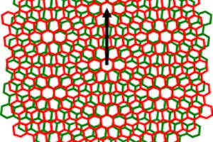
The two graphene sheets are aligned so one sheet is rotated by 11.3 degrees. With a specific laser energy, instead of heating up like any "normal" material - it cools down. The researchers explain that the photons of the laser absorb the vibration energy of the atoms - instead of the other way around.

Read the full story Posted: Sep 17,2014

Allied Market Research: the graphene material market will reach $149.9 million by 2020

Allied Market Research released a new graphene market report in which they analyze graphene opportunities and forecast the market from 2013 to 2020. According to Allied, the global graphene market will grow to $149.1 million by 2020 - a 44% yearly CAGR from 2014.

The electronics and automotive industries will be among the top consumers of graphene in the near future, and Allied sees 1,800 tons of bulk graphene and 26.8 million square-cm of graphene films to be produced and used by 2020. In the products market, GNP was the largest revenue generating segment in 2013 and is expected to retain its position throughout 2014 - 2020. Other promising segments are graphene oxide and monolayer & bi-layer graphene.

Read the full story Posted: Sep 17,2014

Graphene Frontiers partners with CNSE on a $5 million graphene fabrication project

In July 2014, Graphene Frontier launched the "six sensors" brand for highly-sensitive chemical and biological GFET-based sensors following a financing round of $1.6 million. Graphene Frontiers announced a partnership with the Colleges of Nanoscale Science and Engineering (CNSE) at SUNY Polytechnic Institute (SUNY Poly) to develop next generation graphene-based processes, technologies, and techniques.

Graphene Frontiers G-FET sensor

As part of the partnership, Graphene Frontiers and the CNSE will build a 300 mm fabrication process and wafer-transfer facility. The total investment in this project will reach $5 million over 3 years (and will be funded by the CNSE and Graphene Frontiers) and the project will employ 27 employees.

Read the full story Posted: Sep 17,2014

Carbon Sciences to help develop natural gas to graphene process at UCSB

Carbon Sciences logoCarbon Sciences signed an agreement with the University of California, Santa Barbara (UCSB) to fund the further development of a graphene production process developed at the University. This process produces large-area graphene sheets.

The process transforms natural gas into commercial size sheets of graphene that can be fine-tuned with application-specific electrical and materials properties. That's all we know at this stage.

Read the full story Posted: Sep 16,2014

Researchers manage to synthesize Germanene for the first time

Researchers from Europe managed to successfully synthesize germanene - a 2D material that is similar to graphene and made from Germanium atoms. The material was first propose in 2009, but now it was finally realized.

Back in 2009 it was suggested that Germanene can be made by high-temperature deposition in a ultra-high vacuum environment. But the breakthrough in this research came when they used gold as a substrate. An independent group from China also managed to synthesize germanene - and they have used a platinum substrate (which is more expensive than the thin gold films used in the European research).

Read the full story Posted: Sep 16,2014

Electrons in a graphene superlattice behave like in no other material

Manchester University's graphene Nobel laureate Sir Andre Geim, together with Leonid Levitov from MIT discovered that electrons in a graphene superlattice move at a controllable angle to applied fields - this is like sailboats that sail diagonally to the wind.

A graphene superlattice is made from a sheet of graphene aligned on top of a sheet of boron nitride. This material behave as a semiconductor (unlike graphene itself which is a superconductor). The researchers found that the electrons in the new material behave as neutrinos that acquired a notable mass. This effect has no known analog in particle physics.

Read the full story Posted: Sep 13,2014

Graphene Nanochem announce 5-year offtake agreement with Scomi for 135,000 tonnes of graphene-enhanced materials

In November 2013, Graphene Nanochem signed an agreement with Malaysia's Scomi Oiltools, a global supplier of drilling fluid services, to exclusively market a range of formulated graphene-enhanced PlatDrill series to the oilfield chemicals market.

Now Graphene Nanochem signed a licensing and offtake agreement for the entire production of PlatDrill under the Scomi-Platinum joint venture. The two companies will build a 45,000 tonnes per annum (tpa) production facility: 30,000 tpa of Platdrill material and 15,000 of specialty chemicals. The fab will also produce graphene nanomaterial (will increase NanoChem's capacity from 30 tonnes per year to 50). Scomi Oiltools agreed to buy the whole production of PlatDrill over five years (estimated at 135,000 tonnes) with an option to renew for another 5 years.

Read the full story Posted: Sep 13,2014

New method developed to self-assemble GNRs with a zigzag edge

Researchers from Japan's Tohoku University develop a new bottom-up way to produce defect-free graphene nanoribbons (GNRs) with periodic zigzag-edge regions. Using this method, one can control the GNRs' growth direction and length distribution.

Current bottom-up processes use inert substrates - like gold or silver, and this completely determines the way the graphene molecules are assembled, and cannot create zigzag-edge GNRs. The new method uses a copper substrate - which is more reactive then gold or silver. This introduces new substrate-to-molecule interactions, in addition to the intermolecular interactions.

Read the full story Posted: Sep 12,2014

IBM suggests using graphene as a reusable substrate for semiconductor growth

IBM developed a new method to use graphene as a substrate for single-crystalline semiconductor film growth. Graphene will be less expensive than current single-crystalline wafers used in such production methods, as it can be reused indefinitely.

IBM says that growing a 4" GaN film today requires a 4" SiC substrate wafer which is destroyed using the process. The SiC costs about $3,000. Graphene can be used to replace the SiC and will be much cheaper in the long run. Graphene is also useful as it is flexible and can be better adapted for films that need to be transferred to a flexible substrate.

Read the full story Posted: Sep 12,2014

Graphene 3D Lab aims to have commercial graphene-based 3D printing materials in 6 months

Dr. Elena Polyakova photoUsing graphene as a 3D printing material is a very hot topic lately, with many companies attempting to unlock this market - including Graphene 3D Lab, Graphene Technologies, Grafoid, AGT, Qingdao Unique Products and others.

Graphene 3D Lab, a joint-venture between Graphene Labs and Lomiko Metals which recently went public in Canada, is one of the leaders in this new market. The company's founder and COO, Dr. Elena Polyakova, was kind enough to explain the company's technology and business and answer a few questions I had.

Read the full story Posted: Sep 12,2014