A new method of making magnetic graphene that keeps its electronic properties

Researchers at the University of California at Riverside found a way to introduce magnetism in graphene while still preserving electronics properties. This may represent a significant step forward in the use of graphene in chips and electronics, since doping in the past induced magnetism but damaged graphene's electronic properties. this method can also be used in spintronics - chips that use electronic spin to store data.

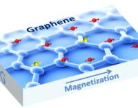
The scientists explain they have overcome the problem by moving a graphene sheet very close to an electrical insulator with magnetic properties, since placing graphene on an insulating magnetic substrate can make the material ferromagnetic without disturbing its conductivity. The magnetic graphene is said to acquire new electronic properties, and so new quantum phenomena can take place.

Read the full story Posted: Jan 27,2015

Polish scientists find way to make super-strong graphene sheets

Researchers at the Polish Lodz University of Technology developed a metallurgical method for producing graphene, that supplies graphene sheets of superior strength. The method relies on liquid metallic matrix and carburising gas mixture and delivers what the researchers call "HSMG" - High Strength Metallurgical Graphene.

The scientists claim this product has a higher strength and repeatability of the physico-chemical properties under varying pressure and temperature conditions, compared to currently produced graphene. They further explain that since they make graphene on liquid metal (that has a flat surface), the structure continuity is maintained and grants strength. 

Read the full story Posted: Jan 27,2015

KAIST develops a novel graphene transfer method

Researchers at the Korean KAIST developed a technique for the delamination of single-layer graphene from a metal etching, that enables different types of transfer methods such as transfer onto a surface of a device or a curved surface, and large surface transfer onto 4 inch wafers. This method could be helpful for wearable smart gadgets and various graphene electronic devices.

While the traditional method of wet transfer might harm or contaminate the graphene in the process, this technique grants safer transfer as well as significant freedom in the transfer process. After a graphene growth substrate formed on a catalytic metal substrate is treated in an aqueous PVA solution, a PVA film is formed and a strong adhesion force is formed between the substrate and the graphene layers. The graphene is delaminated from the growth substrate by means of an elastomeric stamp while the graphene layer is in an isolated state and thus can be freely transferred onto a circuit board.

Read the full story Posted: Jan 26,2015

Chinese LeaderNano launches first phase of Graphene Industrial Park

The Chinese LeaderNano recently launched its first graphene production line that can produce 2-3 tons of graphene powder a year, as part of the first phase of the company’s graphene industrial park.

Phase 1 is planned to grow to include 10 powder production lines and improve capacities of graphene products: goals are set at around 30 tons of graphene powder a year, 150 tons of graphene oxide powder, 1,000 tons of graphene pulp and 1,000 tons of graphene anticorrosive paint. In addition, the industry park will produce 5 to 7 kinds of multi-function special graphene according to demand of different industries, and capacity for each variety may be 3-5 t/a.

Read the full story Posted: Jan 26,2015

Controlling edge properties of graphene nanoribbons

Researchers at Rice University managed to prove it possible to determine the edge properties of graphene nanoribbons by controlling the conditions under which the GNRs are pulled apart. The line-up of atoms along the edges of GNRs determines its properties - metallic or semi-conducting. These properties bear great importance for various applications, electronics being among the leading ones.  

The Rice scientists used computer modeling to demonstrate that it is possible to pull apart nanoribbons and get graphene with either pristine zigzag edges or "reconstructed zigzags" (referring to the process by which graphene atoms are shifted around to form connected rings of five and seven atoms). 

Read the full story Posted: Jan 25,2015

Unique encapsulation may advance graphene devices

Researchers from AMO GmbH and Graphenea SE demonstrated a unique encapsulation technique that enables highly reproducible operation of graphene devices in normal atmosphere for several months. This encapsulation may help in solving one of the major problems of graphene-based devices - sensitivity to environmental elements like humidity or gases.


Read the full story Posted: Jan 22,2015

Graphene Frontiers' employees, Steve Misewicz, passed away at the early age of 29, the company launched a memorial fund

One of Graphene Frontiers' employees, Steve Misewicz, has recently passed away at the early age of 29. Steve was a fabrication engineer at Graphene Frontiers, following his studies at Millersville University. He leaves behind his pregnant wife, Yoonjoo (Jane); his two and half year old son, Jeremiah; and his five-year-old pitbull, Red.

Steve Misewicz photo

Graphene Frontiers launched a memorial fund for Steve Misewicz, aiming to raise $12,000 to support Steve's family.

Read the full story Posted: Jan 21,2015

Graphene's optoelectronic properties enable electrically controlling light at the nanometer scale

Scientists from ICFO, MIT, CNRS, CNISM and Graphenea collaborated to demonstrate how graphene can enable the electrical control of light at the nanometer level. Electrically controlled modulation of light emission is crucial in applications like sensors, displays and various optical communication system. It also opens the door to nanophotonics and plasmonics-based devices. 

The researchers managed to show that the energy flow from erbium into photons or plasmons can be controlled by applying a small electrical voltage. The plasmons in graphene are unique, as they are very strongly confined, with a plasmon wavelength that is much smaller than the wavelength of the emitted photons. As the Fermi energy of the graphene sheet was gradually increased, the erbium emitters went from exciting electrons in the graphene sheet, to emitting photons or plasmons. The experiments showed the graphene plasmons at near-infrared frequencies, which may be beneficial for communications applications. In addition, the strong concentration of optical energy offers new possibilities for data storage and manipulation through active plasmonic networks.

Read the full story Posted: Jan 21,2015

Up close and personal: Roni Peleg

Graphene-Info's personal interviews with industry professionals are a fun way of getting to know the people behind Graphene a bit better. This week's questions will be directed to...me! Roni Peleg, Graphene-Info's senior editor. I would like to take this opportunity and say hello to our readers, and invite people with ideas, questions or comments to feel free to contact the Graphene-Info team.  

Also, If you are a graphene professional of any kind and wish to be featured, contact us here

Roni Peleg, Graphene-Info's senior editor: The way I see it, my job is to make sure our readers get the most interesting, comprehensive and reliable information. So I spend time learning about graphene, reading researches and information from universities, companies and just about anywhere else I can get it. I sift through it to find materials for posts, then write them. I communicate with people from the industry and try to help with anything they need, as well as write in-depth articles about all sorts of graphene topics. I also track news regarding conferences, books, videos and more, so to make sure Graphene-Info stays current and updated. 

Read the full story Posted: Jan 19,2015