Graphene-based imaging technique reveals unprecedented details of nanocrystal structures

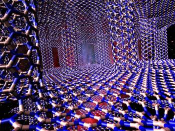
multi-institutional team of researchers led by the U.S. Department of Energy's Lawrence Berkeley National Laboratory (Berkeley Lab) has devised an innovative imaging technique for capturing the 3D structures of nanocrystals, which find application in diverse fields like cancer treatment, pollution reduction, renewable energy collection and more.

The technique, called 3D Structure Identification of Nanoparticles by Graphene Liquid Cell EM (SINGLE), enables the analysis of the 3D structures of these particles for the first time. Metallic nanoparticles have dimensions in the nanometer range, which makes it impossible to visualize their structure. This limitation has prevented researchers from gaining insights into how they work. 
Read the full story Posted: Jul 20,2015

The University at Buffalo receives an $800,000 grant from the Navy to work on graphene-based next-gen power technology.

The University at Buffalo has received an $800,000 grant from the Navy to work on graphene-based next-generation power technology. The Office of Naval Research grant will fund UB engineers' work on the development of nanoribbons of graphene. Buffalo University says the project comes as the Navy seeks alternatives to conventional power control systems.

The Buffalo scientists will strive to desogn complex simulations that examine how graphene nanoribbons can be used as a power switch, explore how adding hydrogen and other elements (a process known as doping) to graphene nanoribbons could improve their performance, and investigate graphene nanoribbons’ failure limit under high power loads and try to find ways to improve it. All of this should be done in the course of the next four years.

Read the full story Posted: Jul 20,2015

On the way to breaking the terahertz barrier for graphene nanoelectronics

A team of scientists at the Max Planck Institute for Polymer Research (MPI-P) discovered that electrical conduction in graphene on the picosecond timescale is governed by the same basic laws that describe the thermal properties of gases. This understanding might allow scientists and engineers not only to better understand but also to improve the performance of graphene-based nanoelectronic devices.

The researchers found that the energy of ultrafast electrical currents passing through graphene is very efficiently converted into electron heat, making graphene electrons behave just like a hot gas. It appears that the heat is distributed evenly over all electrons, and the rise in electronic temperature, caused by the passing currents, in turn has a strong effect on the electrical conduction of graphene.

Read the full story Posted: Jul 20,2015

Nanorods on graphene perform as excellent photocatalyst

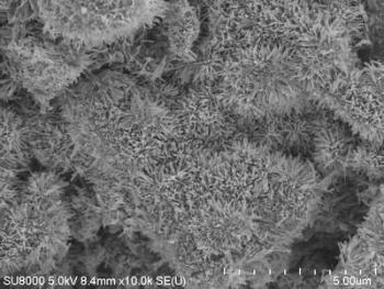
Scientists from the Institute of Physical Chemistry of the Polish Academy of Sciences in Warsaw and Fuzhou University in China developed an innovative photocatalytic material from zinc oxide nanorod arrays grown on a graphene substrate and "decorated" with dots of cadmium sulphide. In the presence of solar radiation, the material showed to be a great catalyst for chemical reactions. 

The material adheres to the principles to photocatalytics, in which radiation (both visible and ultraviolet) is used to activate chemical compounds and carry out reactions which store solar energy. This newly created photocatalyst operates quite simply; when a photon with the appropriate energy meets the semiconductor, an electron-hole pair forms. Under normal circumstances it would almost immediately recombine and the solar energy would be lost. However, in the new material electrons - released in both semiconductors as a result of interaction with the photons - quickly flow down along the nanorods to the graphene base, which is an excellent conductor. Recombination can not occur and the electrons can be used to create new chemical bonds and thus to synthesize new compounds. The actual chemical reaction takes place on the surface of the graphene, previously coated with the organic compounds which are to be processed. 

Read the full story Posted: Jul 20,2015

3D "White graphene" could cool electronics

Researchers at Rice University developed a theoretical model that shows how a 3D lattice of boron nitride (also known as "white graphene" as it shares many similar qualities with it, but is not made of carbon atoms) could be deployed as a tunable material to control heat flow in electronic devices. Cooling measures that prevent overheating in electronics are important for developing and sustaining advanced electronic components.

Its 3D structure allows the speculated boron nitride system to conduct heat in any direction as opposed to most circuits, in which heat moves in one direction. The multiple heat directing properties of boron nitride provide excellent opportunities to ‘cool’ down electronic devices. This can be controlled further by building pillars of boron nitride of differing shapes and thickness.

Read the full story Posted: Jul 20,2015

NRL scientists use graphene in tunnel barrier/transport channel for future spintronic devices

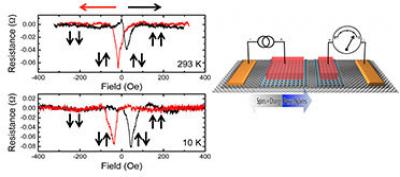
Scientists at the U.S. Naval Research Laboratory (NRL) have created a new type of room-temperature tunnel device structure in which the tunnel barrier and transport channel are both made of graphene. Such functionalized homoepitaxial structures can be seen as an elegant approach for realization of graphene-based spintronic devices.

The scientists show that hydrogenated graphene acts as a tunnel barrier on another layer of graphene for charge and spin transport. They demonstrate spin-polarized tunnel injection through the hydrogenated graphene, and lateral transport, precession and electrical detection of pure spin current in the graphene channel. The team further reports higher spin polarization values than found using more common oxide tunnel barriers, and spin transport at room temperature.

Read the full story Posted: Jul 15,2015

Haydale and Versarien announce collaboration agreement

Haydale has announced a collaboration with Versarien (main owners of 2-DTech) to accelerate the development of their respective graphene projects. The companies will work together to create solutions for the manufacturing and functionalization of graphene on a large scale suitable for mass produced commercial applications.

The companies expect to share resources to maximize the exposure and utilization of the expertise of both organisations, which operate in different areas. In particular, Versarien through its subsidiary 2-D Tech will supply high quality graphene platelets for functionalization using Haydale’s proprietary technology. Haydale will also supply high quality sustainable graphite for use as feedstock by 2-D Tech and evaluate the resulting material.

Read the full story Posted: Jul 15,2015

Oxford scientists design a method that produces large graphene crystals in a matter of minutes

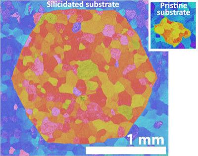
Researchers at Oxford University demonstrated how millimeter-sized crystals of high-quality graphene can be made in minutes instead of hours. In about 15 minutes, the method can produce large graphene crystals (around 2-3 millimeters in size) that it would otherwise take up to 19 hours to produce using current chemical CVD techniques.

The researchers took a thin film of silica deposited on a platinum foil which, when heated, reacts to create a layer of platinum silicide. This layer melts at a lower temperature than either platinum or silica, creating a thin liquid layer that smooths out nanoscale 'valleys' in the platinum so that carbon atoms in methane gas brushing the surface are more inclined to form large flakes of graphene.

Read the full story Posted: Jul 15,2015

Strong piezoelectricity in single-layer graphene could enable graphene-based sensors and electronics

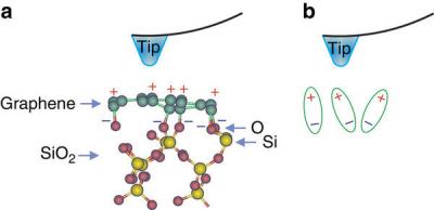
Researchers at the University of Aveiro, Portugal, the Institute of Natural Sciences, Russia and the Instituto de Fisica, Brazil observed a strong piezoelectric activity of single-layer graphene (SLG) deposited on Si/SiO2calibration grating substrates. The scientists perceive the piezoelectric effect to be strong enough to enable future applications like graphene-based actuators, sensors and other electronic components based on the direct and converse piezoelectric effects.  

The researchers performed an experimental study of single-layer graphene (SLG) deposited on SiO2 calibration grating substrates by piezoresponse force microscopy (PFM) and confocal Raman spectroscopy. Piezoelectric activity was mainly observed on the supported graphene regions where van der Waals and/or chemical interaction between the SiO2 surface and graphene layer can induce an anisotropic strain and detectable PFM signal. The piezoelectric activity in the graphene layers was attributed to the chemical interaction of graphene atoms with underlying oxygen from SiO2 substrate. Piezoelectric effect was found to be relatively high, more than twice that of the best piezoelectric ceramics such as modified lead zirconate titanate.

Read the full story Posted: Jul 15,2015

Advanced Graphene Products to develop graphene-based yacht components

Advanced Graphene Products logoThe Polish graphene producer Advanced Graphene products (AGP) and Lodz University of Technology have launched a joint project to produce flexible graphene components for yachts. They plan to develop a technology that will rely on fibre-graphene components that will allow to reduce the weight of various elements while preserving, and even increasing their strength and elasticity.

The plan is for AGP to make yacht components from high strength metallurgical graphene, an enforced material patented by the Polish company. It is a graphene produced on a thin layer of metal that can easily be processed and transferred to other surfaces.

Read the full story Posted: Jul 14,2015