Graphene grown from tea tree extract shows great promise

Scientists at James Cook University in Queensland, Australia, and collaborators from institutions in Australia, Singapore, Japan, and the US have developed a new technique for growing graphene from tea tree extract. Graphene is only made of carbon atoms, so theoretically can be grown from any carbon source, but scientists are still looking for a graphene precursor and growth method that is sustainable, scalable, and economically feasible, since these are all requirements for realizing widespread commercialization of graphene-based devices.

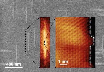
In this study, the researchers have grown graphene from the tea tree plant Melaleuca alternifolia, a plant used to make essential oils in traditional medicine. They demonstrated that it is possible to fabricate large-area, nearly defect-free graphene films from tea tree oil in as little as a few seconds to a few minutes, whereas current growth methods usually take several hours. Unlike current methods, the new method also works at relatively low temperatures, does not require catalysts, and does not rely on methane or other nonrenewable, toxic, or explosive precursors.

Read the full story Posted: Aug 21,2015

Understanding graphene's affinity towards water may open the door to tailored coatings

Scientists at The National Physical Laboratory's (NPL) have been investigating the hydrophobicity of epitaxial graphene, which could be used in the future to better tailor graphene coatings to applications in medicine, electronics and more. Contrary to popular beliefs, the scientists' findings indicate that graphene's hydrophobicity is strongly thickness-related, with single-layer graphene being significantly more hydrophilic than its multi-layered graphene.

As graphene-based devices will have to operate in ambient conditions with existing (and unmonitored) humidity, it may be troublesome that such conditions can affect graphene's performance through changes in its mechanical and electrical properties; The new study, conducted in collaboration with the Naval Research Laboratory, addresses the question of whether graphene is hydrophobic or hydrophilic. The common assumption is that graphene is hydrophobic, but it seems that the results of this study prove the question more complex than previously thought.

Read the full story Posted: Aug 21,2015

Rice scientists embed metals into LIG to benefit fuel cells and supercapacitors

Scientists from Rice University have managed to embed metallic nanoparticles into their previously-developed LIG (laser-induced graphene, a flexible film with a surface of porous graphene made by exposing a common plastic to a commercial laser-scribing beam), that turn the material into a catalyst for fuel cells and various other applications.

The researchers have now found a way to enhance the product with reactive metals and turn it into "metal oxide-laser induced graphene" (MO-LIG), a new candidate to replace expensive metals like platinum in catalytic fuel-cell applications in which oxygen and hydrogen are converted to water and electricity. The scientists state that a major advantage of this process is that commercial polymers can be used, with the addition of inexpensive metal salts. They are then subjected to the laser scriber, which generates metal nanoparticles embedded in graphene. In effect, the laser generates graphene in the open air at room temperature.

Read the full story Posted: Aug 21,2015

New project focuses on graphene-based inks for lighting applications

A collaborative Innovate UK project called Project Graphted that began on 1st April 2015 aims at evaluating Graphene’s potential as a transparent electrode when dispersed in a polymeric matrix. Graphted will be led by PolyPhotonix, a UK-based company that develops applications based on OLED lighting panels, and will include a 12 month feasibility study in which PolyPhotonix will be working in collaboration with Applied Graphene Materials and CPI (a UK-based R&D institute that helps companies develop and scale manufacturing processes).

The project seeks to provide proof of concept evidence that a Graphene-based electronic device can be successfully developed and fully categorised in terms of morphology and physical properties. If so, the approach holds potential to generate a range of electronic inks that can be utilised on a large scale. Application areas include OLEDs and organic photovoltaics (OPV).

Read the full story Posted: Aug 21,2015

Will Black phosphorus with tunable band gap supersede graphene?

A team of scientists from Pohang University of Science and Technology (POSTECH) managed to tune black phosphorus' band gap to form a superior conductor, allowing for the application to be mass produced for electronic and optoelectronics devices.

The tunable band gap in BP effectively modifies the semiconducting material into a unique state of matter with anisotropic dispersion. This research outcome potentially allows for great flexibility in the design and optimization of electronic and optoelectronic devices like solar panels and telecommunication lasers.

Read the full story Posted: Aug 17,2015

Talga moves to eliminate distractions on its way to becoming a graphene supplier

Talga Resources, the Australia-based miner company with gold assets in Australia and high-grade graphite resource in Sweden, announced giving options to sell three gold mining sites, as it aims to focus on graphite and graphene opportunities "without distraction".

Talga owns five high-grade graphite projects in Norrbotten Country in north Sweden, and has not kept its ambitions to become a leading supplier of bulk graphene a secret. The company stated that it would invest the money it received from the sale of these options to resource its graphite and graphene projects in Sweden and Germany.

Read the full story Posted: Aug 17,2015

A novel method forms graphene out of buckyballs

Scientists at the Trento Institute for Fundamental Physics and Applications in Italy have found a way to make graphene using buckyballs as a starting point. The idea of using buckyballs as a precursor for graphene is not new, but a problematic one since the only way to get them to unzip and bind together is to heat them to temperatures in excess of around 600 °C. These high temperatures can change the properties of the substrate, in particular the amount of carbon it adsorbs, so the results are irregular films with serious defects.

Their idea is to bombard the substrate with buckyballs travelling at supersonic speeds, fast enough to get them to open when they hit and the resulting unzipped cages then bond together to form a graphene film. The technique bypasses the usual problems - the team accelerates the buckyballs by releasing them into a helium or hydrogen gas which they allow to expand at supersonic speeds, carrying the carbon balls with it. That gives the buckyballs energies of around 40 keV without changing their internal dynamics (unlike ordinary heating which dramatically increases the molecular vibrations). They then aim the buckyballs at a copper sheet and let them smash into it, resulting in a fairly even coating of graphene-like material in a single layer.

Read the full story Posted: Aug 13,2015

Graphene 3D Lab acquires former parent company Graphene Laboratories

Graphene 3D Lab announced that it will be acquiring all of the issued and outstanding shares of Graphene Laboratories, their former parent company. Graphene Laboratories was originally with aims of developing graphene into a multi-use material suitable for a wide variety of applications.

Graphene 3D Lab will thus acquire an extensive existing client base and profitable retail operation that they will continue to run, and will also hold the provisional patent for a low-energy, chemical-free graphene manufacturing process. This will join the four US patent applications that Graphene 3D Lab currently has pending for its graphene technology.

Read the full story Posted: Aug 13,2015

A technique for growing graphene nanoribbons on semiconductors may lead to more efficient electronics

Researchers at the University of Wisconsin-Madison have discovered a way of growing graphene nanoribbons with desirable semiconducting properties directly on a conventional germanium semiconductor wafer. This finding may allow manufacturers to easily use graphene nanoribbons in hybrid integrated circuits, which promise to deliver a major boost to the performance of next-gen electronic devices. This technology could also have specific uses in industrial and military applications, such as sensors that detect specific chemical and biological species and photonic devices that manipulate light.

The technique for producing graphene nanoribbons is said to be scalable and compatible with the prevailing infrastructure used in semiconductor processing - nanoribbons that can be grown directly on the surface of a semiconductor like germanium are more compatible with planar processing used in the semiconductor industry, and so would pose less of a barrier to integrating these materials into electronics in the future.

Read the full story Posted: Aug 12,2015