February 2016

Graphene impressions from the Mobile World Summit

Last week Barcelona hosted the Mobile World Congress trade show, and it was a very large and impressive conference - with over 100,000 visitors and thousands of exhibiting companies. This year the MWC included a graphene pavilion, organized by the ICFO and the Graphene Flagship, Europe's $1 billion research project initiative.

The Graphene Pavilion was very impressive, with several companies showcasing real graphene products and prototype devices, and also several research groups from leading Universities. The Pavilion consisted of 11 companies and 9 research centers - and you could see graphene materials, graphene supercapacitors (From Zap&Go, soon to hit the market), large graphene EMI shielding films (from GNext), graphene sensors and graphene-based RFID tags and antennas. In the photo below you can see an air quality prototype sensor made from graphene developed by Libre SRL (PiAndBi).
Read the full story Posted: Feb 29,2016

New hexagonal 2D material may rival graphene

Researchers from the University of Kentucky working in collaboration with scientists from Daimler in Germany and the Institute for Electronic Structure and Laser (IESL) in Greece have reported a new (theoretical) 2D material that could potentially rival graphene as the material of the future. The new material is made up of silicon, boron and nitrogen — all light, inexpensive and abundant elements — and is extremely stable, a property many other graphene alternatives lack.

While there are many ways to combine silicon, boron and nitrogen to form planar structures, only one specific arrangement of these elements resulted in a stable structure. The atoms in the new structure are arranged in a hexagonal pattern, as in graphene. The three elements forming the material all have different sizes; the bonds connecting the atoms are also different. As a result, the sides of the hexagons formed by these atoms are unequal, unlike in graphene.

Read the full story Posted: Feb 29,2016

Cornell researchers design chiral graphene

Scientists at Cornell University have developed a chiral thin film through rotational stacking of graphene sheets, the first such exploration of chirality at the nano scale. This material may be of interest in the fields of polarization optics, stereochemistry, optoelectronics and spintronics.

For the experiment,the researchers grew graphene sheets on copper, then cut them into multiple sheets. Those sheets were then stacked, with each sheet rotated slightly before being placed on the one below it. The rotation went clockwise on one stack and counter-clockwise on the other to form right-handed and left-handed stacks. Circularly polarized light alternating left-handed and right-handed beams were shone onto the stacks, and circular dichroism (or CD, the differential absorption of left- and right-handed light), was measured.

Read the full story Posted: Feb 29,2016

Allied Market Research predicts that the world graphene market will Reach $151.4 Million By 2021

A new market report by Allied Market Research projects that the global sales of graphene would reach $151.4 million by 2021, and that the graphene nanoplatelets (GNPs) segment will account for about two-thirds of the overall market revenue by that year. The energy storage application segment is expected to grow at the highest CAGR of 93.2% during the analysis period.

AMR foresees that heavy investment to improve production capacity and focus on strengthening R&D activities would lead to the development of novel and innovative products. Monolayer and bilayer graphene would emerge as lucrative segments, registering a CAGR of 41.5% during 2014 and 2021. The growth of this segment is attributed to its potential applications in electronics, energy storage, 3D printing, and other industries.

Read the full story Posted: Feb 29,2016

Moth-inspired graphene becomes more light and heat absorbing

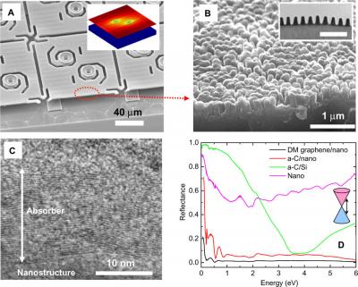
UK-based scientists from BAE Systems and the University of Surrey have discovered that patterned graphene sheets, inspired by moths’ eyes, could be used to capture light to produce energy or power sensors, and could also be used to develop smart wallpaper capable of powering Internet of Things applications.

The researchers claim that the newly developed material is the most light-absorbent substance for its weight developed to date, and drastically improves the efficiency of traditional graphene. They explain that graphene typically absorbs just 2.3% of incidental light; However, their new version of the material could collect as much as 90% more waste light and heat to produce more energy. The difference is a new technique which grows graphene around a textured metallic surface.

Read the full story Posted: Feb 28,2016

Promising graphene-based component achieved using a new, simple method

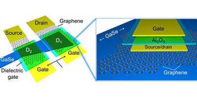
Researchers at Aalto University in Finland have fabricated an electricity-conducting material with promising properties by merging graphene and another 2D material, gallium selenide. The newly designed heterojunction could prove important for applications like sensors and wearable electronics and are, in comparison similar components that contain silicon, extremely thin. They also have impressive properties and the method used for their preparation is simpler than previous researched methods.

The component structure utilized elements from both lateral and vertical device design enabling the use of standard fabrication methods utilized in the semiconductor industry instead of laborious manual fabrication. The scientists explain that their inspiration comes from the existing silicon technology, aiming to bring out the state-of-the-art fabrication of 2D material devices from research labs to industry. In addition to the new and simpler way of manufacturing, the components have excellent characteristics like the on/off ratio, which is a critical parameter in electronics - over 10³.

Read the full story Posted: Feb 21,2016

CPI's Graphene Centre now open for business

The Centre for Process Innovation (CPI) has opened the doors of a Graphene Centre that aims to help companies develop, prove and commercialize products using graphene technologies. The Graphene Centre was funded by Innovate UK to support the commercial growth of the UK graphene industry and operates two specialized facilities at NETPark in Sedgefield, County Durham.

It has a dedicated laboratory for the functionalization and characterization of Graphene at a significant scale, which is produced by a variety of process routes. The second facility is based in CPI’s printable electronics facility and is focused on device development and testing covering membranes, sensors, energy and electronic applications.

Read the full story Posted: Feb 18,2016

Thomas Swan receives government grants for two development projects

Thomas Swan, manufacturer of performance and specialty chemicals, has announced that it has received funding from Innovate UK, the UK’s innovation agency, for two new collaborative projects in a program entitled Advancing the Commercial Applications of Graphene. Both projects are due to start on 1st April 2016.

One of the projects involves a collaboration between Thomas Swan Advanced Materials and Plessey Semiconductors, Nano Products and Nottingham Trent and Strathclyde universities on flexible LEDs. The other project will see Thomas Swan cooperating with DelStar International, Haydale, and the University of Bradford to develop plastic composites for advanced separations.

Read the full story Posted: Feb 18,2016

BCC Research sees a bright future for graphene

A recent BCC Research report predicts that between 2015 and 2025, the graphene market will achieve unprecedented growth rates through technological advancements, spotting increasing patent activity that suggests that technology trends are under way, ripening the market for explosive future growth.

BCC Research expects a commercially significant market for graphene products to develop between 2015 and 2020, when the market is projected to be worth more than $310.4 million. The graphene market will supposedly continue to grow rapidly after 2020, approaching $2 billion by 2025.

Read the full story Posted: Feb 17,2016

Nanomedical Diagnostics launches a new graphene biosensor

Nanomedical Diagnostics, a biotech company that aims to create practical and scalable graphene biological field effect transistor (BioFET) products, announced the completion of its first AGILE (Automatic Graphene Immunolinked Electronic) biosensor Early Access Development Kit test with a lab at the University of Colorado Anschutz Medical Campus.

The lab needed in vitro protein concentration measurements to validate its RNA data, but doing so using traditional protein analysis methods such as Western Blot was almost impossible due to the amount of tissue required to observe the protein. The AGILE platform reportedly provided quantitative, reproducible protein concentration data in one afternoon. One of the professors from the University of Colorado Anschutz Medical Campus declared that This technology is a game-changer for developmental biologists and that It opens the field of proteomics to a discipline that’s previously used just RNA data because it was cost-prohibitive to gain the quantity of protein needed for detection on traditional platforms.

Read the full story Posted: Feb 17,2016