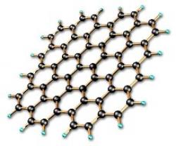
There are various methods to produce graphene materials, such as mechanical exfoliation of graphite, liquid-phase exfoliation and reduction of graphene oxide (GO), each with its own set of advantages and disadvantages. Chemical vapor deposition (CVD) is a method of producing graphene that has attracted much attention in the last decade and despite several shortcomings, is considered a leading approach to manufacture graphene, especially for applications like high-performance electronics and sensors, as it can yield high quality graphene sheets with a low defect count and good uniformity.
The CVD process
Generally speaking, the CVD method is based on gaseous reactants that are deposited on a substrate. The graphene is grown on a metallic surface like Cu, Pt or Ir, after which it can be separated from the metal and transferred to specifically-required substrates. When the gases contact the substrate inside the heated reaction chamber, a reaction occurs that creates a film of material on the substrate. The process can be simply explained as carbon-bearing gases that react at high temperatures (900â1100â°C) in the presence of a metal catalyst, which serves both as a catalyst for the decomposition of the carbon species and as a surface for the nucleation of the graphene lattice.
As was mentioned before, conditions like temperature, pressure, duration of time and many more can have a significant influence on the process and so must be carefully monitored.
Advantages and disadvantages
CVD can yield high quality graphene, with common characteristics that may include high homogeneity, imperviousness, high purity, fine grains, good control over layer number and more. However, CVD also comes with several disadvantages - namely a relatively high price of the equipment, toxic gaseous by-products and, as stated before, it is a rather sensitive process that is easily influenced by parameter changes. It is important to note that while CVD is a rather expensive method compared to other methods to produce lower-quality graphene, it is still probably the best way (to date) to acquire high quality graphene, since other ways to do that are even more expensive or complicated.
In addition, the separation (or exfoliation) of graphene from the substrate is known as challenging and it is tricky to accomplish without damaging the structure of the graphene or affecting the properties of the material. Another harrowing task is the creation of a uniform layer of graphene on a substrate, something that is continuously proving to not be easy at all.
Some approaches were and are still being developed to overcome this issue, like modifying the concentration of gases and incorporating spin coating methods, but this remains a challenge. However, despite these challenges, it is important to note that CVD is widely considered as an important and promising method to produce graphene, which is already in use, and will probably be even more so in the future, once further advancements are made. It is noteworthy that CVD is already a dominant manufacturing route for many other nanomaterials, and will assumably be in extremely common use once progress is made to resolve the issues that are currently hindering its acceptance.
Market status
While using the CVD method to produce graphene is definitely one the leading approaches in the world, it is still hindered by the challenges mentioned above. Thus, it is currently mostly limited to relatively small volumes and mainly restricted to R&D and academic uses.

However, graphene sheets produced via CVD methods are used in several applications like sensors, touch screens and heating elements. It is believed that once better answers are found to the questions of price and handling of CVD graphene, many more applications will start to appear.
Looking to buy CVD graphene sheets?
If you are interested in buying CVD graphene sheets, check out the Graphene Catalog that lists various CVD produced graphene sheets from several producers.
The latest CVD graphene news:
Graphene Biosensor Evolution: From devices on silicon to lower cost, more flexible biodegradable plastic
This is a guest-post by Jeffrey Draa, CEO at Grolltex - producing graphene biosensors on silicon chips today shows low yields, high cost and restrictive packaging options, limiting scalability and market penetration. But optimization may be here.
Monolayer, electronics grade graphene is propelling advanced biosensing in many key areas. Google the search term, ‘graphene biosensor’, and one will see thousands of next-generation, life enhancing applications being refined in research labs worldwide. This one atom thick material is creating biosensing and detection performance in speed and sensitivity not possible before. Areas such as cancer and virus detection, new drug discovery, genomics, allergens, glucose and many more are starting to see unimagined advances. By far, the number 1 use case for monolayer graphene films today is atomic level biosensing.
Researchers succeed in creating single-crystal, large-area, fold-free monolayer graphene
A team of researchers, led by Director Rod Ruoff at the Center for Multidimensional Carbon Materials (CMCM) within the Institute for Basic Science (IBS) and including graduate students at the Ulsan National Institute of Science and Technology (UNIST), has achieved growth and characterization of large area, single-crystal graphene totally free from wrinkles, folds, or adlayers. It was said to be 'the most perfect graphene that has been grown and characterized, to date'.
Director Ruoff notes: This pioneering breakthrough was due to many contributing factors, including human ingenuity and the ability of the CMCM researchers to reproducibly make large-area single-crystal Cu-Ni(111) foils, on which the graphene was grown by chemical vapor deposition (CVD) using a mixture of ethylene with hydrogen in a stream of argon gas. Student Meihui Wang, Dr. Ming Huang, and Dr. Da Luo along with Ruoff undertook a series of experiments of growing single-crystal and single-layer graphene on such ‘home-made’ Cu-Ni(111) foils under different temperatures.
Graphenea Foundry: a platform for the manufacture of graphene-based devices
This is a sponsored post by Graphenea
Graphenea’s Semiconductor catalogue spans from 1x1 cm2 single layer graphene films on a variety of substrates, to fully customized graphene-based device architectures implemented on wafers up to 150mm. The unique vertical integration that Graphenea offers, that covers the graphene growth, its transfer, its device fabrication and post-processing, allows Graphenea to have full control of the manufacturing process, continuously monitoring this through quality control processes and checkpoints.
")
Graphenea Foundry offers three products and services, which cover all the graphene needs one may have.
CharmGraphene starts mass producing CVD graphene using a roll-to-roll process
Korea-based Charmgraphene has started to mass produce CVD graphene, using its proprietary roll-to-roll process.
 CharmGraphene's graphene on copper and heating element
CharmGraphene's R2R production system can produce 2 meters of CVD graphene per minute (maximum width 300 mm). According to CharmGraphene, its current CVD graphene capacity is about 8,000 sqm per month. The company says it uses use 6 um thick copper foil which reduces copper foil etching time dramatically compare to 35 um thickness copper foil used by other companies.
Graphene-Info updates all its graphene market report
Today we published new versions of all our graphene market reports. Graphene-Info provides comprehensive niche graphene market reports, and our reports cover everything you need to know about these niche markets. The reports are now updated to July 2021.
The Graphene Batteries Market Report:
- The advantages using graphene batteries
- The different ways graphene can be used in batteries
- Various types of graphene materials
- What's on the market today
- Detailed specifications of some graphene-enhanced anode material
- Personal contact details into most graphene developers
The report package provides a good introduction to the graphene battery - present and future. It includes a list of all graphene companies involved with batteries and gives detailed specifications of some graphene-enhanced anode materials and contact details into most graphene developers. Read more here!
POSCO sets out to establish a graphene ecosystem to meet growing demand
South Korea's leading steel group, POSCO, will reportedly lead the creation of a graphene ecosystem in the southeastern industry port of Pohang in cooperation with research groups and Graphene Square, to meet the growing demand in the fields of semiconductors, electronics, electric batteries and composites.
POSCO said it has signed a business agreement with Pohang City, the Research Institute of Industrial Science & Technology (RIST), Pohang University of Science and Technology (POSTECH), and Graphene Square, which is developing systems for the mass production of large-scale graphene synthesized by chemical vapor deposition (CVD).
Introducing: The CVD Graphene Market Report
Graphene-Info is proud to present our new market report, The CVD Graphene Market Report. This market report, brought to you by the world's leading graphene industry experts, is a comprehensive guide to CVD graphene materials, the current industry and market status, and the promising applications in optoelectronics, bio-sensors, thermal solutions and more.
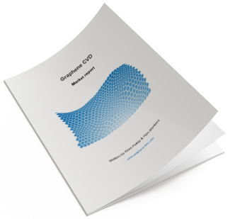
Reading this report, you'll learn all about:
- How does CVD graphene differ from other graphene types
- CVD graphene properties
- Possible applications for CVD graphene
- Available materials on the market
The report also provides a list of prominent CVD graphene research activities, a list of all CVD graphene developers and their products, datasheets and brochures from over 10 different CVD graphene makers and more.
Graphene Square prepares for IPO and aims for mass production of CVD graphene
![]() South Korea-based Graphene Square, developer and distributor of graphene materials and films, has announced that it is preparing for an IPO to fuel global expansion. It will select the underwriter this year and plans its Kosdaq listing in 2022 through the Technology Special Listing program, a system introduced in 2005 to allow promising startups to list the local bourse based on a technology evaluation conducted by Korea Exchange-designated institutions.
South Korea-based Graphene Square, developer and distributor of graphene materials and films, has announced that it is preparing for an IPO to fuel global expansion. It will select the underwriter this year and plans its Kosdaq listing in 2022 through the Technology Special Listing program, a system introduced in 2005 to allow promising startups to list the local bourse based on a technology evaluation conducted by Korea Exchange-designated institutions.
Graphene Square’s competitive edge is said to be found in its proprietary chemical vapor deposition (CVD) method used for the production of graphene. The method is based on the research of Professor Hong Byung-hee of Seoul National University on the synthesis of large-area graphene. In fact, Graphene Square itself was established in 2012 as a spin-off of chemistry professor Hong Byung-hee’s lab at Seoul National University.
An interview with planarTECH's CEO to discuss the company's future roadmap and plans
UK-based planarTECH has concluded a successful equity crowdfunding campaign in 2020, as part of Graphene-Info's Graphene Crowdfunding Arena. We posted a post-campaign interview with the company's CEO, J. Patrick Frantz back in June 2020. We thought it was time to get an update as things are moving fast for the company.

Hello Patrick! It's been over half a year since you concluded the successful crowdfunding campaign. What are your thoughts now regarding the process and the campaign?
The crowdfunding was definitely an interesting experience and we’re glad we did it. It is hard for us to say if our experience was normal or not due to our campaign being launched at the beginning of the first wave of the COVID-19 pandemic. In the end, however, we did reach our stated goal, though we didn’t get quite enough funding to do the things we really want to do. As a result, we're still considering bringing on new investment, and for this round we are looking at more traditional fundraising methods (strategic partners, etc.).
A graphene industry, market and new conference series interview with Dr. Khasha Ghaffarzadeh
Our friend Dr. Khasha Ghaffarzadeh, a well respected graphene market analyst, is launching a new service called TechBlick that is a subscription-based online and all-year round event focused on advanced materials such as graphene, 2D materials, CNTs, boron nitrides, QDs, and more.
Graphene-Info partnered with TechBlick, to provide our readers an exclusive 25% discount on the TechBlick subscription. We took advantage of this launch to discuss the graphene market and industry with Dr. Ghaffarzadeh and also discuss the new service.
Hello Kasha. How do you see the graphene market shaping up in 2021?
I have closely followed and examined the graphene industry for a full decade. The landscape has certainly changed. Many companies have come and gone, and many once considered revolutionary applications are now ruled out, but overall, the industry is now at a tipping point.
We think 2021/2022 will be a turning point, setting the industry on its growth path, despite the delays caused these past 12 months due to Covid. For some, these delays have been painful as projects were pushed back or partners or customers dropped graphene to focus on other core areas. Many undershot their growth expectations, and some had difficult cash flow situations.