Researcher from Columbia University demonstrated that it is possible to electrically contact an atomically thin graphene (or any 2D material) only along its edge (rather than contacting it from the top). This new architecture enabled a new assembly technique that prevents interface contamination. This new assembly process resulted in the cleanest graphene ever made. They say that the new edge-contact geometry actually provides a more efficient contact without the need for complex processing.
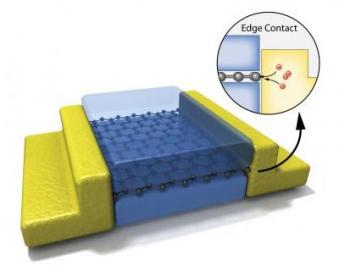
This research work solved two graphene problems - contamination and contact. Having contacts just at the edges virtually eliminates external contamination. To achieve this breakthrough, the researchers fully encapsulated a single graphene sheet in a sandwich of thin insulating boron nitride crystals, employing a new technique in which crystal layers are stacked one-by-one.
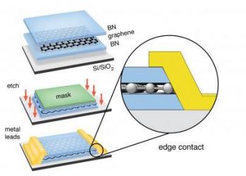
This stack was then etched to expose the edge and then metal was evaporated onto the edge to create the electrical contact. Even though the electrons entered only at the edge of the graphene sheet, the contact resistance was remarkably low, reaching 100 Ohms per micron of contact width.
This new stacking assembly method and the contact architecture allowed the team to produce what they say is the cleanest graphene ever made. They say that the electron mobility is at least twice as large as any conventional 2D electron system and the sheet resistivity is less than 40 Ohms when sufficient charges are added to the sheet by electrostatic "gating."


The researchers are now applying these techniques to develop new hybrid materials by mechanical assembly and edge contact of hybrid materials such as graphene, boron nitride, transition metal dichlcogenides (TMDCs), transition metal oxides (TMOs), and topological insulators (TIs). They say that potential applications include vertically structured transistors, tunneling based devices and sensors, photoactive hybrid materials, flexible and transparent electronics and more.