Spiraling laser pulses find graphene's on/off switch

Scientists from the Department of Energy’s SLAC National Accelerator Laboratory and the Stanford Institute for Materials and Energy Sciences (SIMES) collaborated to study the effects of spiraling pulses of laser light on graphene. They discovered that such spiraling laser pulses can theoretically change the electronic properties of graphene, switching it back and forth from a metallic state (where electrons flow freely), to an insulating state.

Such ability could mean that it is possible to use light to encode information in a computer memory, for instance. The study, while theoretical, attempted to work in as close-to-real experimental conditions as possible, right down to the shape of the laser pulses. The team found that the laser's interaction with graphene yielded surprising results, producing a band gap and also inducing a quantum state in which the graphene has a so-called Chern number of either one or zero, which results from a phenomenon known as Berry curvature and offers another on/off state that scientists might be able to exploit.
Read the full story Posted: May 28,2015

FlexEnable details their graphene OTFT goals

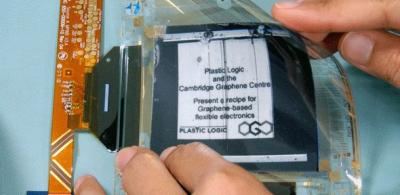
UK-based FlexEnable was spun-off from Plastic Logic in February 2015 with an aim to further develop and commercialize the company’s technology platform for organic thin film transistor (OTFT) arrays for flexible displays and ubiquitous sensing. Last month FlexEnable joined the graphene flagship, and announced plans to develop new use cases for graphene in flexible electronics.

I talked briefly to Mike Banach, FlexEnable's Technical Director, and he explained the company's graphene plans and goals. FlexEnable is not a material company - they do not aim to develop and produce graphene material. The define themselves as a applied process technology - what we call a graphene application developer, focused on the flexible electronics market.

Read the full story Posted: May 17,2015

Rice scientists find simple ways to control graphene QDs from coal

Back in 2013, Rice scientists developed a simple method to reduce coal into graphene quantum dots (GQDs). Now, these Rice researchers have found a way to engineer these GQDs for specific semiconducting properties in two separate processes.

The researchers' work demonstrates precise control over the graphene oxide dots' band gap, the very property that makes them semiconductors. By sorting the QDs through ultrafiltration, it was found possible to produce quantum dots with specific semiconducting properties. The second process involved direct control of the reaction temperature in the oxidation process that reduced coal to quantum dots. The researchers found hotter temperatures produced smaller dots that had different semiconducting properties. The dots in these experiments came from treatment of anthracite, a kind of coal. The processes produce batches in specific sizes between 4.5 and 70 nanometers in diameter.

Read the full story Posted: Mar 23,2015

Stamp-printing folds into graphene

Researchers at Trinity College Dublin invented a rubber-stamp printing method (GraFold) to introduce waves into graphene, in a simple and large-scale way. The printing process is done using computer modelling to show the behavior of the graphene films on the stamp and substrate, and the wavy graphene can be printed onto any type of surface allowing for more sophisticated investigations of its properties.

In this transfer printing process called GraFold, the excess graphene required for forming the folds is induced by using PDMS stamps with a relief pattern such that the graphene tension and adhesion is modulated across the stamp. The graphene is kept on a planar structure at first, then the supporting polymer is dissolved and the graphene layer can ease into the recessed patterns. The graphene inked stamp is then placed gently onto the destination substrate, and then the stamp is peeled away leaving the mechanically patterned graphene film attached to the substrate.

Read the full story Posted: Feb 17,2015

Scientists identify novel 2D semiconductors arsenene and antimonene

Researchers from the Institute of Optoelectronics & Nanomaterials at Nanjing University of Science and Technology used density functional theory computations to identify novel 2D wide band gap semiconductors called arsenene and antimonene.

The materials are typical semimetals in their natural layered state. However, monolayered arsenene and antimonene are indirect wide band gap semiconductors, and under strain they become direct band-gap semiconductors. Scientists believe that such dramatic transitions of electronic properties could bring new possibilities for nanoscale transistors with high on/off ratio, optoelectronic devices and sensors based on new ultrathin semiconductors.

Read the full story Posted: Jan 14,2015

Scientists discover a way to manipulate graphene nanoribbons and reach precise structural control

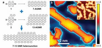
Researchers at the US Department of Energy's (DOE) Lawrence Berkeley National Laboratory (Berkeley Lab) and the University of California, Berkeley, have developed a new approach for synthesizing graphene nanoribbons from pre-designed molecular building blocks. Using this process the researchers built nanoribbons that have enhanced properties (tunable bandgaps, for example) that can be potentially useful for advanced electronics.

Read the full story Posted: Jan 12,2015

Electrons in a graphene superlattice behave like in no other material

Manchester University's graphene Nobel laureate Sir Andre Geim, together with Leonid Levitov from MIT discovered that electrons in a graphene superlattice move at a controllable angle to applied fields - this is like sailboats that sail diagonally to the wind.

A graphene superlattice is made from a sheet of graphene aligned on top of a sheet of boron nitride. This material behave as a semiconductor (unlike graphene itself which is a superconductor). The researchers found that the electrons in the new material behave as neutrinos that acquired a notable mass. This effect has no known analog in particle physics.

Read the full story Posted: Sep 13,2014

Researchers fabricate graphene-like TGCN for the first time

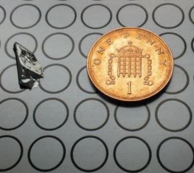
Researchers from the University of Liverpool managed to fabricate, for the first time, a new 2D material called triazine-based graphitic carbon nitride, or TGCN. TGCN is similar to graphene but it has a band gap.

To produce the TGCN, the researcher started with dicyandiamide. They then created crystals of graphitic carbon nitride (a 2D material). Both materials were combined in a quartz tube and heated for 62 hours (at 600 degrees Celsius). The resulting liquid contains TGCN flakes.

Read the full story Posted: May 22,2014

Visible light can be used to dope graphene-BN heterostructures

Researchers from Berkeley Lab and the University of California (UC) Berkeley developed a method to open a bandgap in a graphene boron-nitride (GBN) heterostructure using visible light. Using this so called "photo-induced doping" of the GBN the researchers created pn junctions and other useful doping profiles while preserving the material’s remarkably high electron mobility.

Using visible light is very promising as this technique is very flexible and (unlike electrostatic gating and chemical doping) does not require multi-step fabrication processes that reduce the graphene's quality. Using this method, one can make and erase different patterns easily.

Read the full story Posted: May 19,2014

Growing graphene on hexagonal BN opens a bandgap

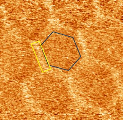
Researchers from the University of Manchester demonstrated that when growing graphene on a hexagonal substrate (hBN, or hexagonal Boron-Nitride, in that case), small changes in the crystal structure can open a band-gap in the graphene. The researchers also demonstrated that a graphene grown on the hBN can exist in an alternative structure in which the band gap is much smaller.

The lattice structure of hBN (also called white graphene) is quite similar to graphene. When you place the graphene on top of the hBN, a moiré superlattice is created. The periodic potential associated with this superlattice causes a number of new and interesting electronic phenomena to occur in graphene, including Hofstadter's butterfly, which has been shown before.

Read the full story Posted: May 09,2014