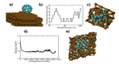
Graphene quantum dots and TiO2 exhibit fascinating light harvesting capabilities

Researchers at Australia's Griffith University have discovered a fascinating mechanism, that may allow the design of a new class of composite materials for light harvesting and optoelectronics. The team has found a quantum-confined bandgap narrowing mechanism, where UV absorption of the graphene quantum dots and TiO2 nanoparticles can easily be extended into the visible light range.

According to the scientists, real life application of this would be high efficiency paintable solar cells and water purification using sun light. In addition, the team states that "this mechanism can be extremely significant for light harvesting. What's more important is we've come up with an easy way to achieve that, to make a UV absorbing material to become a visible light absorber by narrowing the bandgap."

Read the full story Posted: Jul 20,2016

NRL designs low-defect method to nitrogen dope graphene resulting in tunable bandstructure

A team of scientists at the U.S. Naval Research Laboratory (NRL) has demonstrated hyperthermal ion implantation (HyTII) as an effective means of doping graphene with nitrogen atoms. The result is a low-defect film with a tunable bandstructure that could be useful in a variety of device platforms and applications.

According to the research, the HyTII method delivers a high degree of control including doping concentration and, for the first time, demonstrates depth control of implantation by doping a single monolayer of graphene in a bilayer graphene stack. This further demonstrates that the resulting films have high-quality electronic transport properties that can be described solely by changes in bandstructure rather than the defect-dominated behavior of graphene films doped or functionalized using other methods.

Read the full story Posted: Jun 07,2016

A novel approach to interconnecting GNRs could lead to high-performance graphene-based electronics

An international team of researchers at Tohoku University in Japan has demonstrated the ability to interconnect graphene nanoribbons (GNRs) end to end, using molecular assembly that forms elbow structures (interconnection points). This development may provide the key to unlocking GNRs’ potential in high-performance and low-power-consumption electronics.

GNRs are interesting as their width determines their electronic properties; Narrow ones are semiconductors, while wider ones act as conductors, which basically  provides a simple way to engineer a band gap into graphene for use in electronics.

Read the full story Posted: Jan 14,2016

Manipulating graphene's wrinkles could lead to graphene semiconductors

Researchers at Japan's RIKEN have discovered that wrinkles in graphene can restrict the motion of electrons to one dimension, forming a junction-like structure that changes from zero-gap conductor to semiconductor back to zero-gap conductor. Moreover, they have used the tip of a scanning tunneling microscope to manipulate the formation of wrinkles, opening the way to the construction of graphene semiconductors by manipulating the carbon structure itself in a form of "graphene engineering."

The scientists were able to image the tiny wrinkles using scanning tunneling microscopy, and discovered that there were band gap openings within them, indicating that the wrinkles could act as semiconductors. Two possibilities were Initially considered for the emergence of this band gap. One is that the mechanical strain could cause a magnetic phenomenon, but the scientists ruled this out, and concluded that the phenomenon was caused by the confinement of electrons in a single dimension due to "quantum confinement."

Read the full story Posted: Oct 26,2015

Graphene nano-coils could replace solenoids for miniature electronics

Researchers at Rice University found that graphene nano-coils possess natural electromagnetic properties and can help in scaling down electronics by possibly replacing common solenoids (wires coiled around a metallic core that produce a magnetic field when carrying current, turning them into electromagnets. Solenoids also serve as inductors, primary components in electric circuits that regulate current, and in their smallest form are part of integrated circuits). 

The researchers discovered that when a voltage is applied, current will flow around the helical path and produce a magnetic field, as it does in macro inductor-solenoids. These graphene coil-structures are even found to form naturally during graphite growth, so they don't require complicated configuration or assembly. The researchers believe it should be possible to isolate graphene coil formations from crystals of graphitic carbon (graphene in bulk form), but enticing graphene sheets to grow in a spiral would allow for better control of its properties. 

Read the full story Posted: Oct 17,2015

A novel method of opening a band gap in graphene allows for high-performance transistors

Researchers at Sungkyunkwan University and the Institute for Basic Science in Suwon, South Korea have designed a new method for opening up a band gap in graphene to allow the construction of graphene-based transistors.

In this study, the scientists have opened a band gap in graphene by carefully doping both sides of bilayer graphene in a way that avoids creating disorder in the graphene structure. Delicately opening up a band gap in graphene in this way enabled the researchers to fabricate a graphene-based memory transistor with the highest initial program/erase current ratio reported to date for a graphene transistor (34.5 compared to 4), along with the highest on/off ratio for a device of its kind (76.1 compared to 26), while maintaining graphene's naturally high electron mobility (3100 cm2/V·s).

Read the full story Posted: Sep 23,2015

IDTechEx's analyst explains his views on the graphene market

Dr Khasha Ghaffarzadeh, IDTechExA few weeks ago we reported on a new IDTechEx market report, in which they predict that the graphene market will reach nearly $200 million by 2026, with the estimation that the largest sectors will be composites, energy applications and graphene coatings.

We were very interested in learning more, and Dr Khasha Ghaffarzadeh, IDTechEx's head of consulting was kind enough to answer a few questions and explain the company's view on the graphene market.

Q: IDTechEx has been following graphene for a long time with dedicated events and reports. Why is this new material interesting for IDTechEx?

We have a long track record of analyzing emerging advanced materials such as quantum dots, CNTs, Ag nanostructures, silicon nanostructures, OLED materials, etc. We were however pulled into the world of graphene by our clients’ questions. Once in, we soon realized that there is a big synergy between graphene and our events. in fact, our events on supercapacitors and printed electronics were the right near-term addressable market for graphene, and that is why we managed to rapidly build up the largest business-focused event on graphene. Our events on graphene are held in the USA and Europe each year see www.IDTechEx.com/usa.

Read the full story Posted: Sep 04,2015

GNRs undergo successful boron-doping for possible sensor applications

Scientists at the University of Basel have managed to synthesize boron-doped graphene nanoribbons and characterize their structural, electronic and chemical properties. The modified material could potentially be used as a sensor for ecologically damaging nitrogen oxides.

Altering graphene sheets to nanoribbon shape is known as a way of inducing a bandgap, whose value is dependent on the width of the shape. To tune the band gap in order for the graphene nanoribbons to act like a silicon semiconductor, the ribbons usually undergo doping. That means the researchers intentionally introduce impurities into pure material for the purpose of modulating its electrical properties. While nitrogen doping has been realized, boron-doping has remained unexplored. Subsequently, the electronic and chemical properties have stayed unclear thus far.

Read the full story Posted: Aug 29,2015

Will Black phosphorus with tunable band gap supersede graphene?

A team of scientists from Pohang University of Science and Technology (POSTECH) managed to tune black phosphorus' band gap to form a superior conductor, allowing for the application to be mass produced for electronic and optoelectronics devices.

The tunable band gap in BP effectively modifies the semiconducting material into a unique state of matter with anisotropic dispersion. This research outcome potentially allows for great flexibility in the design and optimization of electronic and optoelectronic devices like solar panels and telecommunication lasers.

Read the full story Posted: Aug 17,2015

A novel method forms graphene out of buckyballs

Scientists at the Trento Institute for Fundamental Physics and Applications in Italy have found a way to make graphene using buckyballs as a starting point. The idea of using buckyballs as a precursor for graphene is not new, but a problematic one since the only way to get them to unzip and bind together is to heat them to temperatures in excess of around 600 °C. These high temperatures can change the properties of the substrate, in particular the amount of carbon it adsorbs, so the results are irregular films with serious defects.

Their idea is to bombard the substrate with buckyballs travelling at supersonic speeds, fast enough to get them to open when they hit and the resulting unzipped cages then bond together to form a graphene film. The technique bypasses the usual problems - the team accelerates the buckyballs by releasing them into a helium or hydrogen gas which they allow to expand at supersonic speeds, carrying the carbon balls with it. That gives the buckyballs energies of around 40 keV without changing their internal dynamics (unlike ordinary heating which dramatically increases the molecular vibrations). They then aim the buckyballs at a copper sheet and let them smash into it, resulting in a fairly even coating of graphene-like material in a single layer.

Read the full story Posted: Aug 13,2015