Electronics

Researchers electrically manipulate a ‘chiral interface state’ in a 2D material

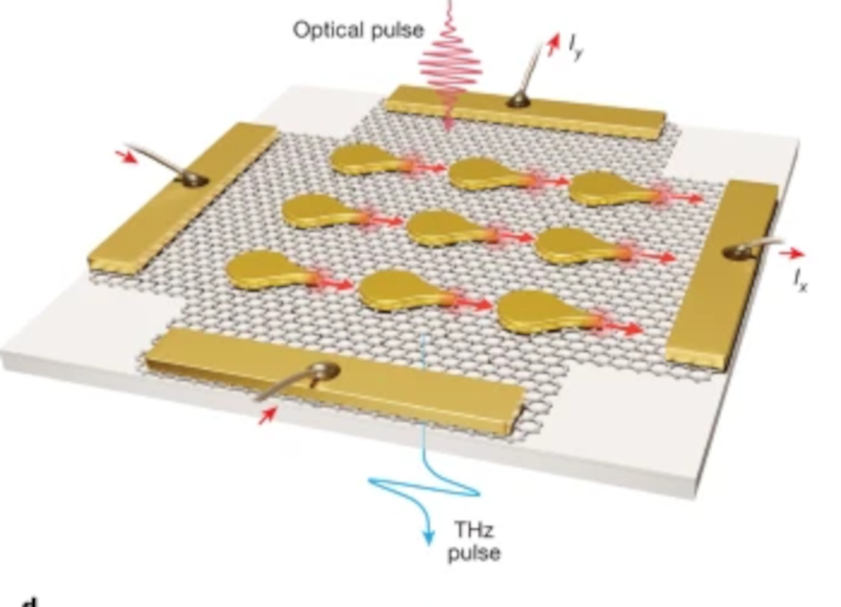
Researchers from  Purdue University, University of California, Lawrence Berkeley National Laboratory and Japan's National Institute for Materials Science have managed to electrically manipulate a ‘chiral interface state’ in twisted monolayer-bilayer graphene, with potential for energy-efficient microelectronics and quantum computing.

The international research team, led by Lawrence Berkeley National Laboratory (Berkeley Lab), has taken the first atomic-resolution images and demonstrated electrical control of a chiral interface state – an exotic quantum phenomenon that could help researchers advance quantum computing and energy-efficient electronics.

Read the full story Posted: Apr 11,2024

Researchers use graphene to develop protective layer for 2D quantum materials

Researchers at the Würzburg-Dresden Cluster of Excellence ct.qmat, along with additional collaborators, have developed a graphene-based protective film that shields quantum semiconductor layers just one atom thick from environmental influences without compromising their quantum properties. This could advance the use of these delicate atomic layers in ultrathin electronic components.

A few years ago, scientists from the Cluster of Excellence ct.qmat discovered that topological quantum materials such as indenene hold great promise for ultrafast, energy-efficient electronics. These extremely thin quantum semiconductors are composed of a single atom layer – in indenene’s case, indium atoms – and act as topological insulators, conducting electricity virtually without resistance along their edges. Experimental physicist Professor Ralph Claessen explained that producing such a single atomic layer requires sophisticated vacuum equipment and a specific substrate material. To utilize this two-dimensional material in electronic components, it would need to be removed from the vacuum environment. However, exposure to air, even briefly, leads to oxidation, destroying its revolutionary properties and rendering it useless.

Read the full story Posted: Mar 02,2024

Researchers use graphene to develop new metasurface architectures for ultrafast information processing and versatile terahertz sources

Traditional microelectronic architectures are currently used to power everything from advanced computers to everyday devices. However, scientists are always on the lookout for better technologies. Recently, Los Alamos National Laboratory scientists and their collaborators from Menlo Systems and Sandia National Laboratories, have designed and fabricated asymmetric, nano-sized gold structures on an atomically thin layer of graphene. The gold structures are dubbed “nanoantennas” based on the way they capture and focus light waves, forming optical “hot spots” that excite the electrons within the graphene. Only the graphene electrons very near the hot spots are excited, with the rest of the graphene remaining much less excited.

Illustration of an optoelectronic metasurface consisting of symmetry-broken gold nanoantennas on graphene. Image from Nature

The team adopted a teardrop shape of gold nanoantennas, where the breaking of inversion symmetry defines a directionality along the structure. The hot spots are located only at the sharp tips of the nanoantennas, leading to a pathway on which the excited hot electrons flow with net directionality — a charge current, controllable and tunable at the nanometer scale by exciting different combinations of hot spots. 

Read the full story Posted: Feb 08,2024

Researchers develop self-assembling graphene sensors for modular wearable electronics

Researchers at Peking University, University of Science and Technology Beijing and Peking University Third Hospital have reported magnetically self-assembling graphene sensors. 

While wearable sensors can provide continuous, personalized health tracking beyond clinical visits, most devices today still have fixed designs targeting single applications, lacking versatility to address users' changing needs. The team's recent work could address this issue and enable modular, reconfigurable wearable electronics customized to individuals. 

Read the full story Posted: Jan 29,2024

Researchers develop novel graphene-based implantable neurotechnology

A new study, led by the Catalan Institute of Nanoscience and Nanotechnology (ICN2) along with the Universitat Autònoma de Barcelona (UAB) and other international partners like the University of Manchester (under the European Graphene Flagship project), presents EGNITE (Engineered Graphene for Neural Interfaces) - a novel class of flexible, high-resolution, high-precision graphene-based implantable neurotechnology with the potential for a transformative impact in neuroscience and medical applications. 

This work aims to deliver an innovative technology to the growing field of neuroelectronics and brain-computer interfaces. EGNITE builds on the experience of its inventors in fabrication and medical translation of carbon nanomaterials. This innovative technology based on nanoporous graphene integrates fabrication processes standard in the semiconductor industry to assemble graphene microelectrodes of a mere 25 µm in diameter. The graphene microelectrodes exhibit low impedance and high charge injection, essential attributes for flexible and efficient neural interfaces.

Read the full story Posted: Jan 15,2024

Researchers succeed in creating graphene-based functional semiconductor

Researchers at the Georgia Institute of Technology and China's Tianjin University have created a novel functional semiconductor made from graphene, potentially opening the door to various next-gen electronics. 


This discovery comes at a time when silicon, the material from which nearly all modern electronics are made, is reaching its limit in the face of increasingly faster computing and smaller electronic devices. The semiconductor made from graphene is compatible with conventional microelectronics processing methods – a necessity for any viable alternative to silicon.

Read the full story Posted: Jan 05,2024

Researchers examine brucite/graphene composites for improved electronics

Researchers at the University of Bologna have introduced and considered a single layer of brucite Mg(OH)2, a 2D material that can be easily produced by exfoliation (like graphene from graphite), for the creation of van der Waals composites (known as heterostructures, or heterojunctions), where two monolayers of different materials are stacked and held together by dispersive interactions. 

First principles simulations showed that brucite/graphene composites can modify the electronic properties (position of the Dirac cone with respect to the Fermi level and band gap) according to the crystallographic stacking and the presence of point defects. This could be meaningful for various applications, such as electronics. 

Read the full story Posted: Dec 31,2023

Copper-graphene composites could lead to better electrical wires and motors

Researchers at North Carolina State University and Pacific Northwest National Laboratory have found that graphene can enhance an important property of metals called the temperature coefficient of resistance. 

They showed that mixing graphene in just the right proportion with copper could lead to improved electrical wires for more efficient electricity distribution to homes and businesses, as well as more efficient motors to power electric vehicles and industrial equipment. The team has applied for a patent for the work, which was supported by the Department of Energy (DOE) Advanced Materials and Manufacturing Technologies Office.

Read the full story Posted: Dec 21,2023

Researchers use ultrafast lasers to map ballistic movement of electrons in graphene

Researchers at the University of Kansas’ Ultrafast Laser Lab have observed the ballistic movement of electrons in graphene in real time. 

Image credit: University of Kansas

“Generally, electron movement is interrupted by collisions with other particles in solids,” said lead author Ryan Scott, a doctoral student in KU’s Department of Physics & Astronomy. “This is similar to someone running in a ballroom full of dancers. These collisions are rather frequent — about 10 to 100 billion times per second. They slow down the electrons, cause energy loss and generate unwanted heat. Without collisions, an electron would move uninterrupted within a solid, similar to cars on a freeway or ballistic missiles through air. We refer to this as ‘ballistic transport.’”

Read the full story Posted: Dec 16,2023

Researchers turn tiny graphene disks into electromagnets

Researchers from Helmholtz-Zentrum Dresden-Rossendorf, Universität Duisburg-Essen, CENTERA Laboratories, Indian Institute of Technology, University of Maryland and the U.S. Naval Research Laboratory have used graphene disks to demonstrate light-induced transient magnetic fields from a plasmonic circular current with extremely high efficiency. 

The effective magnetic field at the plasmon resonance frequency of the graphene disks (3.5 THz) is evidenced by a strong ( ~ 1°) ultrafast Faraday rotation ( ~ 20 ps). In accordance with reference measurements and simulations, the team estimated the strength of the induced magnetic field to be on the order of 0.7 T under a moderate pump fluence of about 440 nJ cm−2.

Read the full story Posted: Dec 05,2023