Researchers develop graphene-based wearable touch panel for virtual-real handwriting interaction

Researchers from China's Qingdao University and Shenzhen University have developed a graphene-based proof-of-concept for a skin-friendly and wearable textile-based touch panel that converts a person's forearm into a keyboard or sketchpad. The three-layer, touch-responsive material translates what a user sketches or types into computer pictures.

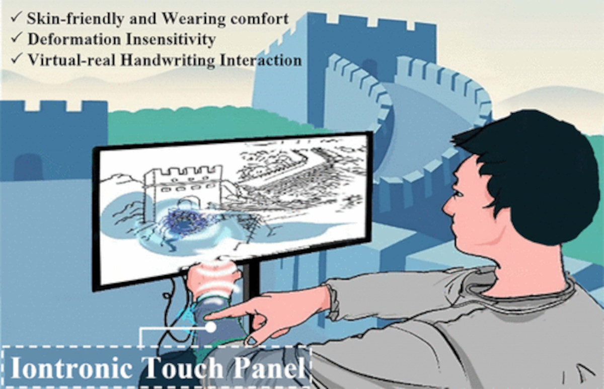
Computer trackpads and electronic signature capture devices are not common in wearables. Researchers have proposed constructing flexible touch-responsive panels out of clear, electrically conductive hydrogels, but these materials are sticky, making writing on them difficult and uncomfortable for the skin. As a result, the research team sought to combine a comparable hydrogel into a comfortable fabric sleeve for drawing or playing computer games.

Read the full story Posted: May 05,2023

Paragraf acquires Cardea Bio, renames it Paragraf USA

UK-based Paragraf has acquired U.S-based Cardea Bio, maker of graphene biosensors. Cardea Bio has been renamed Paragraf USA and Michael Heltzen, CEO and co-founder of Cardea Bio, became EVP of Strategy at Paragraf USA.

“Joining Paragraf allows us to use the world’s only mass-produced, transfer-free monolayer graphene to manufacture the state-of-the art graphene-based biosensors developed by the Cardea team over the last ten years. We are looking forward to unlocking powerful synergistic effects to advance the broad and growing use of graphene biosensors for the benefit of both people and the planet,” says Heltzen.

Read the full story Posted: May 02,2023

Researches develop novel method for building graphene-based nanocircuits with tunable properties

Scientists from CiQUS, ICN2, University of Cantabria, Donostia International Physics Center (DIPC), and Technical University of Denmark (DTU) have joined forces to develop a versatile method for building brick by brick carbon nanocircuits with tunable properties. The team sees this as a significant breakthrough in the precise engineering of 2D materials. The proposed fabrication technique opens exciting new possibilities for materials science, and, in particular, for application in advanced electronics and future solutions for sustainable energy.

The team synthesized a new nanoporous graphene structure by connecting ultra-narrow graphene strips, known as “nanoribbons”, by means of flexible “bridges” made of phenylene moieties (which are portions of larger molecules). By modifying in a continuous way the architecture and angle of these bridges, the scientists can control the quantum connectivity between the nanoribbon channels and, ultimately, fine-tune the electronic properties of the graphene nanoarchitecture. The tunability could also be controlled by external stimuli, such as strain or electric fields, providing opportunities for different applications.

Read the full story Posted: May 01,2023

Researchers study ‘sandwich’ of graphene and boron nitride for next-gen microelectronics

Graphene conducts electricity well – too well, in fact, to be useful in microelectronic technology. But by sandwiching graphene between two layers of boron nitride, which also has a hexagonal pattern, a moiré pattern results. The presence of this pattern is accompanied by dramatic changes in the properties of the graphene, essentially turning what would normally be a conducting material into one with (semiconductor-like) properties that are more amenable to use in advanced microelectronics. But in order to harness this potential for industrial use, there is first a need to better understand the dynamics. 

Researchers from University at Buffalo, Japan's National Institute for Materials Science and Chiba University, Chinese Academy of Sciences (CAS), Thailand's King Mongkut’s Institute of Technology Ladkrabang and Korea's Sungkyunkwan University have chosen a strategy of rapid electrical pulsing to drive carriers in graphene/hexagonal boron nitride (h-BN) heterostructures deep into the dissipative limit of strong electron-phonon coupling. By using electrical gating to move the chemical potential through the “Moiré bands”, they show a cyclical evolution between metallic and semiconducting states. The team's results demonstrate how a treatment of the dynamics of both hot carriers and hot phonons is essential to understanding the properties of functional graphene superlattices. 

Read the full story Posted: Apr 21,2023

Researchers use graphene to design transformable nano-scale electronic devices

Researchers at University of California, Irvine, working with a team from Japan's National Institute for Materials Science, have reported the discovery of nano-scale devices that can transform into many different shapes and sizes even though they exist in solid states. This comes in contrast to conventional nano-scale electronic parts in devices like smartphones, that are solid, static objects that once designed and built cannot transform into anything else. This recent finding could fundamentally change the nature of electronic devices, as well as the way scientists research atomic-scale quantum materials. 

 Schematic of an hBN-encapsulated graphene device with a local graphite back gate and flexible serpentine leads connected to the movable QPC top gates (metal contacts to the graphene and graphite not shown). Image from Science Advances

“What we discovered is that for a particular set of materials, you can make nano-scale electronic devices that aren’t stuck together,” said Javier Sanchez-Yamagishi, an assistant professor of physics & astronomy whose lab performed the new research. “The parts can move, and so that allows us to modify the size and shape of a device after it’s been made.”

Read the full story Posted: Apr 19,2023

Researchers design novel device that combines graphene and high-temperature superconductors

Researchers from the SUNY Polytechnic Institute, Stony Brook University and the Brookhaven National Laboratory in the US, along with Aalto University in Finland, have demonstrated a new electronic device that employs the unique ways in which electrons behave in graphene and high-temperature superconductors.

The experiment, led by Sharadh Jois and Ji Ung Lee from SUNY with the support of theoretical work done by Jose Lado, assistant professor at Aalto, demonstrated a new quantum device that combines both graphene and an unconventional high-temperature superconductor.

Read the full story Posted: Apr 17,2023

Haydale and City Energy develop graphene underfloor heating with Plumbase

Haydale has announced it is working with City Energy Network Limited and Plumbase Limited on developing and distributing its graphene underfloor heating ("UFH").

The ink heater technology applied to clothing worn by British athletes at the Tokyo Games has been applied in an initial prototype for domestic UFH with the potential to replace gas central heating and link into other energy efficient technologies.

Read the full story Posted: Mar 16,2023

Researchers develop graphene/MoS2 micro-electrochemical capacitors for ultra-high charge storage

Researchers from the Indian Institute of Science have developed ultramicro-electrochemical capacitors with two-dimensional (2D) molybdenum disulphide (MoS2) and graphene-based electrodes. The development has great potential for wearables and implantable electronics as well as for sensors and miniature “smart” technology. 

The miniature energy storage device uses graphene Flakes and MoS2 alternately in each electrode - the cathode and anode. Gel was used as the electrolyte, which makes it possible to integrate micro-supercapacitors into chips. This would be difficult if not impossible with a water-soluble electrolyte. The capacitor showed a capacitance of 1.8 mF/cm2 for a single-layer structure (graphene-MoS2). The multilayer electrode structure, consisting of multiple alternating layers of graphene and molybdenum disulfide, gained 30 times greater capacitance, or 54 μF/cm2.

Read the full story Posted: Mar 16,2023

Graphenest partners with Hubron International to explore graphene-based materials for EMI shielding

Graphenest and Hubron recently announced they have entered a strategic partnership to explore the development and commercialization of graphene-based polymer masterbatch and compounds with unprecedented electromagnetic interference (EMI) shielding performance for electronic enclosures manufacturing. 

The companies explained that this new product line will start with a graphene-based thermoplastic suitable to be implemented as a remarkable EMI shielding solution in medium-high and high frequencies (for 5G and beyond).

Read the full story Posted: Feb 26,2023

Researchers develop graphene-nanowire 'sandwich' thermal interface for better electronics

Researchers from Carnegie Mellon University and MIT have demonstrated a 3D graphene-nanowire “sandwich” thermal interface that enables an ultralow thermal resistance of ∼0.24 mm2·K/W that is about 1 order of magnitude smaller than those of solders and several orders of magnitude lower than those of thermal greases, gels, and epoxies.

In addition, the new 3D graphene-nanowire “sandwich” thermal interface also boasts a low elastic and shear moduli of ∼1 MPa like polymers and foams. It exhibits excellent long-term reliability with >1000 cycles over a broad temperature range from −55 °C to 125 °C. This nanostructured thermal interface material can greatly benefit a variety of electronic systems and devices by allowing them to operate at lower temperatures or at the same temperature but with higher performance and higher power density.

Read the full story Posted: Feb 16,2023