Researchers from Rice University and the Oak Ridge National Laboratory (ORNL) found a new method to control the growth of uniform atomic layers of molybdenum disulfide (MDS), a semiconductor together with graphene can be used to make 2D electronic devices. Unlike graphene, MDS has a band gap.
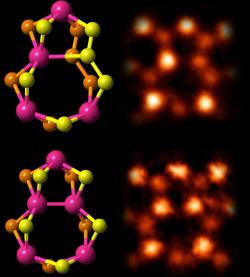
The researchers goal is to create large MDS sheets (using CVD) and then use it together with graphene and the insulator hexagonal boron nitride (hBN) to form field-effect transistors, integrated logic circuits, photodetectors and flexible optoelectronics. MD5 isn't flat - it's actually a stack, with a layer of molybdenum atoms between two layers of sulfur atoms. It's a challenge to actually bind these three materials together.
Normally, when using CVD, it creates small MD5 grains rather then sheets. But the researchers found they could control that nucleation by adding artificial edges to the substrate. Using this technique MD5 grows a lot better, and they report growing grain sizes as large as 100 microns.

