 AMO is a German-based research service provider for material nanofabrication, with competence in nanofabrication, nanoelectronics, nanophotonics and biotechnology.
For the graphene industry, AMO offers CVD graphene materials, graphene device (transistors) fabrication, graphene substrates and more.
Contact information for AMO GmbH
Otto-Blumenthal-Straße 25
52074 Aachen
Germany
Researchers design graphene-based infrared emitter for integrated photonic gas sensors
Researchers at AMO GmbH, KTH Royal Institute of Technology, Senseair AB and the University of Bundeswehr have developed a waveguide-integrated incandescent thermal mid-infrared emitter using graphene as the active material. This innovative approach is said to significantly enhance the efficiency, compactness, and reliability of gas sensor systems, paving the way for widespread applications across various industries.

Many applications require robust, real-time air quality monitoring solutions, driving the demand for distributed, networked, and compact gas sensors. Traditional gas sensing methods, including catalytic beads and semiconducting metal oxide sensors, suffer from performance degradation, frequent calibration needs, and limited sensor lifetimes due to their reliance on chemical reactions. Absorption spectroscopy offers a promising alternative by utilizing the fundamental absorption lines of several gases in the mid infrared (mid-IR) region, including greenhouse gases. This method provides high specificity, minimal drift, and long-term stability without chemically altering the sensor. The ability to “fingerprint” gases through characteristic absorption wavelengths, such as carbon dioxide (CO2) at 4.2 μm, makes it a promising technology for precise gas detection.


Apply today to take part in the Graphene Flagship experimental 2D pilot line!
The Graphene Flagship’s 2D Experimental Pilot Line (2D-EPL) is offering the opportunity to take part in a multi project wafer run integrating graphene into silicon wafers. This run is mainly intended for electronics but can also include sensor devices (e.g. Hall sensor, but via opening on graphene is not in the scope of this run) and will be provided by AMO GmbH. The design of the device can be adjusted within the specifications. Apply today to receive more information or to discuss your design ideas with our team.

- Why apply?
- Affordable prototypes
- Benchmarking
- Customisable chips
- Short turn around
- Flexible process flows
- Direct communication channels
- Experienced partners
- Feasibility consulting
Learn more and apply today!
2D-EPL offers a chance to test graphene-based sensors on large scale
The 2D Experimental Pilot Line (2D-EPL), that originated from the Graphene Flagship, recently launched its first customizable wafer run.
As one of five multi-project wafer (MPW) runs, this first phase is targeting sensor applications. Companies, universities and research institutes can include their designs as dies on joint wafers, to test their ideas for devices on a larger scale at relatively low costs. The first 2D-EPL MPW run opened in February and the call closes on 30 June 2022. The manufacturing stage of the MPW run will take place between 1 September and 31 October 2022.
Metal–Insulator–Graphene diodes enable terahertz rectennas on flexible substrates
Researchers from AMO GmbH, RWTH Aachen University, Chalmers University and the University of Wuppertal have recently developed a novel type of graphene-based flexible energy harvester, which reportedly shows good prospects for powering wearable and conformal devices.
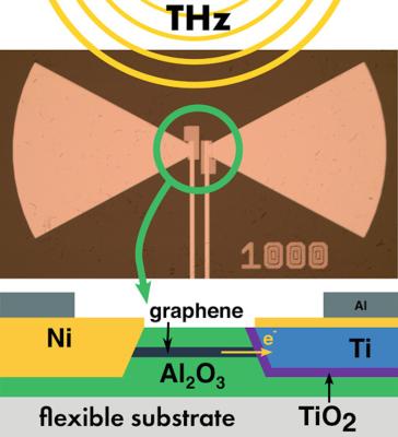
The device is a 'rectenna' - an antenna directly coupled to a diode, which is able to detect radiation and to transform it into a DC output. Rectennas working in the microwave region have been well established since the sixties, thanks to the availability of Schottky diodes with a sufficiently short response time. The challenge is to extend the working principle of rectennas to higher frequency ranges in particular terahertz (THz) and optical frequencies.
Researchers develop smallest graphene-based accelerometer ever reported
Researchers from Sweden and Germany (from KTH Royal Institute of Technology, RWTH Aachen University and Research Institute AMO GmbH, Aachen) have developed the smallest graphene-based accelerometer ever reported. This achievement has been referred to as "a breakthrough for body sensor and navigation technologies".
For the past few decades microelectromechanical systems (MEMS) have been the basis for research and innovations. Now there is a move to the next level nano-electromechanical systems, or NEMS. Xuge Fan, a researcher in the Department for Micro and Nanosystems at KTH, says that the unique material properties of graphene have enabled them to build these ultra-small accelerometers. Based on the surveys and comparisons we have made, we can say that this is the smallest reported electromechanical accelerometer in the world, Fan said.
European team integrated graphene and metal to create waterproof electronic circuits
A team of European researchers from the KTH Royal Institute of Technology, Chalmers University of Technology and Uppsala University in Sweden, along with scientists from RWTH Aachen University and AMO GmbH in Germany, has discovered that when graphene is integrated with the metal of a circuit, contact resistance is not impaired by humidity. This finding may help to develop new sensors with a significant cost reduction.
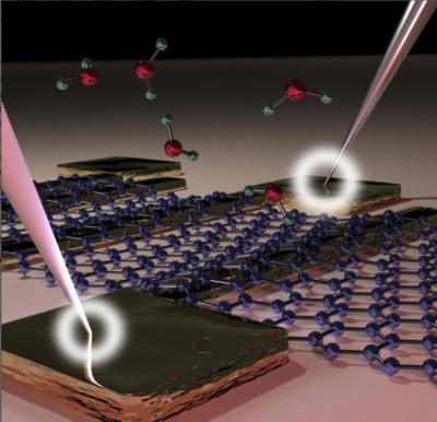
To achieve efficient sensors, graphene needs to make good electrical contacts when integrated with a conventional electronic circuit. Such proper contacts are crucial in any sensor and significantly affect its performance. But a common problem is that graphene is sensitive to humidity, to the water molecules in the surrounding air that are adsorbed onto its surface. The H2O molecules change the electrical resistance of the graphene material, which introduces a false signal into the sensor.
Graphenea, AMO and Emberion to take part in a bringing graphene short-wave infrared (SWIR) detectors to market
Graphenea, AMO and Emberion have been approved a European Innovation Council Fast Track to Innovation (FTI) project to help bring to market the G-IMAGER, a graphene imager based on graphene-on-wafer technology. The G-Imager is a short-wave infrared (SWIR) detector for applications in semiconductor inspection, sorting systems, spectroscopy hyperspectral imaging and surveillance.

A major obstacle for wider use of SWIR imaging products is the high cost of SWIR detectors, which are currently primarily manufactured with InGaAs technology. The high price is related to the complex manufacturing of InGaAs that also prevents increase of the detector production volumes. Now Graphenea Semiconductor SL, Emberion Oy, and AMO GmbH are tasked with constructing and marketing the G-Imager which will bring the core price down significantly, allowing market volumes to grow substantially.
Graphene shows promise for high-speed optical communications
Researchers affiliated with the Graphene Flagship have demonstrated novel high-speed graphene-based data communication at a data rate of 50 Gb/s. Integrating graphene sheets into silicon photonics could form the basis for next-generation data communications.
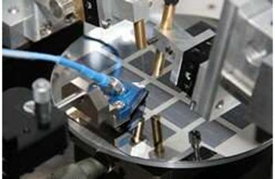
The project was a collaboration between Flagship partners AMO GmbH (Germany), the National Inter-University Consortium for Telecommunications (CNIT) (Italy), Ericsson (Sweden), Ghent University (Belgium), the Institute of Photonic Sciences (ICFO) (Spain), imec (Belgium), Nokia (Germany and Italy), the Vienna University of Technology (TU Wien) (Austria) and the University of Cambridge (UK).
Graphene Flagship team shows the potential of graphene-enhanced photonics
Researchers affiliated with the Graphene Flagship have shown that integrated graphene-based photonic devices offer a unique solution for the next generation of optical communications. Researchers in the initiative have demonstrated how properties of graphene enable ultra-wide bandwidth communications coupled with low power consumption to radically change the way data is transmitted across the optical communications systems. This could make graphene-integrated devices the key ingredient in the evolution of 5G, the Internet-of-Things (IoT), and Industry 4.0.

"As conventional semiconductor technologies are approaching their physical limitations we need to explore entirely new technologies to realize our most ambitious visions of a future networked global society," explains Wolfgang Templ, Department Head of Transceiver Research at Nokia Bell Labs in Germany, which is a Graphene Flagship partner. "Graphene promises a significant step in performance of key components for optical and radio communications beyond the performance limits of today's conventional semiconductor-based component technologies." Paola Galli, Nokia IP and Optical networks Member of Technical Staff, agrees: "Graphene photonics offer a combination of advantages to become the game changer. We need to explore new materials to go beyond the limits of current technologies and meet the capacity needs of future networks."
Graphene Flagship partners design graphene-based phase modulators for faster mobile technology
Graphene Flagship Partners at the National Inter-University Consortium for Telecommunications (CNIT) in Italy, IMEC in Belgium and University of Cambridge in UK have designed and tested a graphene-based phase modulator that reportedly outperforms existing silicon-based ones.
Modern optical data and telecommunications employ phase modulators to increase the amount of data relayed and data rate efficiency, i.e. the speed at which information is relayed. Phase modulators traditionally work by grouping several bits of information into fewer symbols, or packets, reducing the overall size, or spectral width. The smaller the spectral width, the higher the data rate efficiency. However, this efficiency is reaching a maximum with silicon based devices, and so a novel solution is needed to bridge the gap between the increase in demand for data and the efficiency in transmitting it.

