A team of researchers from the University of Cambridge, RWTH Aachen University and the National Institute for Materials Science in Japan has developed a methodology for simultaneously optimizing the growth and the transfer process of graphene, showing that it is possible to dry-transfer graphene with high-yield, if the crystallographic orientation of the growth surface is chosen appropriately.
Graphene often needs to be transferred from the growth substrate (typically copper) to a final substrate where components can be built. However, current transfer approaches either lead to a substantial degradation of the crystal quality or are not compatible with high-volume manufacturing. Moreover, while graphene has great potential for next generation electronics, the gap between the performance of “hero devices” realized in research labs and what can be reproducibly fabricated with scalable approaches remains large. This is why high-end electronic devices enabled by graphene are still not on the market – and why scalability is such a challenge in terms of making the most of this nanomaterial.
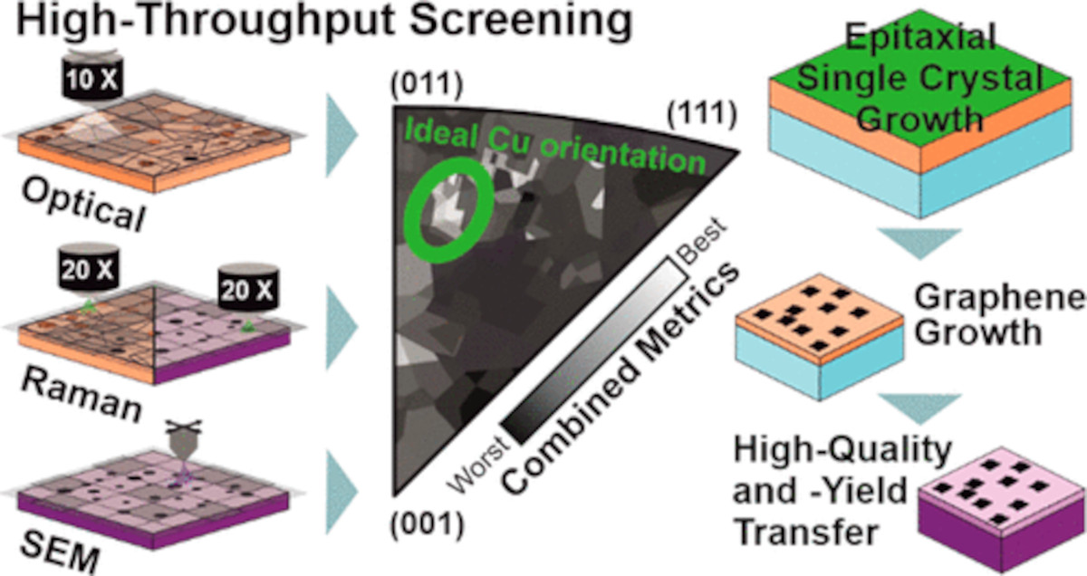
Part of the problem is because, up until now, the growth and transfer of graphene have been treated as two separate processes and optimized independently. Now, the team has developed a high-throughput screening approach that allows for simultaneous optimization of both the growth and the transfer of graphene. Thanks to this method they have been able to demonstrate a scalable pathway for the mechanical transfer of graphene islands grown by CVD. The process ensures both high yield (>95%), and high quality of the graphene domains, with electron mobilities in the range of 40000 cm2/(Vs) at room temperature – a result that might be a real breakthrough for the industrialization of graphene.
“The most challenging aspect of the work was the wealth of data that we generated,” says Oliver Burton, researcher at University of Cambridge and co-lead author of the paper. “We have taken thousands of data points on thousands of individual graphene islands grown on more than 100 different crystal orientations and performed measurements throughout the entire growth and transfer process. The methodology that we have developed to weave all this information together in a meaningful way is one of the most important results of this work. Not only was it was the key to finding a way to transfer CVD graphene with high yield and high quality, but it is also readily adaptable to a wealth of other materials systems.”
Zachary Winter, researcher at RWTH Aachen University and co-lead author of the paper, says, “Within the Graphene Flagship, we could use both of our university’s strengths – Cambridge on material growth and RWTH on device fabrication and characterization – to holistically analyze the parameter space of the whole growth and transfer process. The high-throughput screening approach that we have developed can be the framework for optimizing the growth and transfer of other 2D materials. The next objective is to realize heterostructures all based on CVD-grown materials.”