February 2010

A new nanostructure called Graphene Nanomesh opens up a band gap

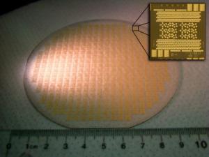
Researchers from UCLA has created a new Graphene nanostructure called Graphene nanomesh (GNM). The new structure is able to open up a band gap in a large sheet of graphene to create a highly uniform, continuous semiconducting thin film that may be processed using standard planar semiconductor processing methods.

The nanomesh can have variable periodicities, defined as the distance between the centers of two neighboring nanoholes. Neck widths, the shortest distance between the edges of two neighboring holes, can be as low as 5 nanometers. This ability to control nanomesh periodicity and neck width is very important for controlling electronic properties because charge transport properties are highly dependent on the width and the number of critical current pathways.

Read the full story Posted: Feb 26,2010

Researchers developed a one step process to enable n- and p-type doping of large area graphene surfaces

Researchers at Georgia Tech say they have developed a one step process that enables both n- and p-type doping of large area graphene surfaces. The used commercially available spin on glass (SOG) material and applied to a sheet of graphene and then exposing it to electron beam radiation. To create both doping types you simply vary the exposure time, with higher levels of energy producing p-type areas.

Read the full story Posted: Feb 23,2010

Angstron to make nanocomposite materials for Nanotek

Nanotek Instruments, parent company of Angstron Materials, has been issued a US Patent for its development of a new high-performing class of meso-porous nanocomposites.  The new nanocomposite provides a superior supercapacitor electrode material for uses that include hybrid electric vehicles (EVs), transportation and energy storage. The technology is based on the company’s breakthrough discovery of nano graphene platelets (NGPs). Angstron, the world leader in production of NGPs, will make the nanocomposite material.

Angstron will provide the meso-porous NGP nanocomposites in two forms: NGPs coated with a thin layer of conducting polymer or surface functional groups and NGPs bonded by a conductive binder, coating, or matrix material such as a polymeric carbon. The platelets in these products are comprised of a sheet of graphite plane or multiple sheets of graphite plane with a thickness less than 10 nm and an average length, width, or diameter smaller than 500 nm. The binder or matrix material bonded to the platelets to form the nanocomposite material create a surface area greater than 500 m.sup.2/gm.

Read the full story Posted: Feb 11,2010

UCSB bought a system for graphene and carbon nanotube growth from Aixtron

Aixtron logoAixtron announced today that it has received a purchase order for a 6" Black Magic Plasma Enhanced CVD (PECVD) system for graphene and carbon nanotube (CNT) growth from the University of California (UCSB).

This combined thermal CVD and plasma enhanced CVD tool is planned to be delivered in first quarter 2010 to Professor Kaustav Banerjee, who directs the Nanoelectronics Research Lab at UCSB. The PECVD system uses unique rapid heating and plasma technologies that is used to produce various types of nanotubes, including low temperature, multiwall, singlewall and supergrowth nanotubes.

Read the full story Posted: Feb 09,2010

Researchers use Graphene to create a new lighting source

Researchers from Sweden and the US have produced a new transparent lighting component that is made from Graphene. They say it is cheap to make and fully recyclable, and might be an alternative to OLED Lighting. The new device is called an Organic Light-emitting Electrochemical Cell, or LEC. The Graphene is used for an electrode. 

LECs can be made using a roll-to-roll process, because all of its parts can be made from liquid solutions.

Read the full story Posted: Feb 06,2010

IBM developed a 100-Ghz Graphene RF Transistor, now works on 1-Thz ones

IBM Research has fabricated new 100-Ghz Graphene RF-transistors on 2" wafers. IBM says that the transistors, which operate at room temperature are the fastest available expect the fastest GaAs transistors, and are more than twice faster than silicon transistors with the same gate length (40Ghz). IBM's next aim is to increase the speed of the Graphene transistor to 1 Thz.

The Graphene RF transistors were created for the Defense Advanced Research Project Agency under its Carbon Electronics for RF Applications (CERA) program. The transistors were fabricated at the wafer scale using epitaxially grown graphene processing techniques that are compatible with those used to fabricate silicon transistors.

Read the full story Posted: Feb 05,2010

Penn State researchers developed a way to make graphene on 100 millimeter wafers

Penn State researchers say that have developed a method of fabricating pure sheets of Graphene on 100 millimeter wafers. They are using silicon sublimation which thermally removes silicon from silicon carbide wafers leaving behind pure graphene. They say that this process can be used to make Graphene chips that are 100 to 1000 times faster than silicon, and also enable other applications such as sensors, displays, solar cells and more.

Read the full story Posted: Feb 02,2010