This is a sponsored post by Graphenea
Graphenea’s Semiconductor catalogue spans from 1x1 cm2 single layer graphene films on a variety of substrates, to fully customized graphene-based device architectures implemented on wafers up to 150mm. The unique vertical integration that Graphenea offers, that covers the graphene growth, its transfer, its device fabrication and post-processing, allows Graphenea to have full control of the manufacturing process, continuously monitoring this through quality control processes and checkpoints.

Graphenea Foundry offers three products and services, which cover all the graphene needs one may have.
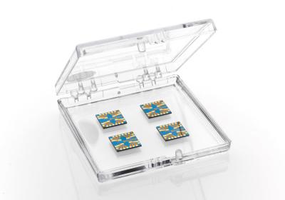
Our GFETs are ready to use, plug & play graphene field effect transistors. There are 2 different device categories;
GFET S1X: These are devices which are considered for general purpose, such as gas sensing, magnetic field sensing, quantum transport experiments, optoelectronics, etc. They come in three different geometries: Hall bars, van der Pauw and interdigitated devices; all the dies have devices with different aspect ratios to explore geometry dependencies in the measurements.
GFET S2X: There are devices dedicated for liquid environments, suitable for biosensing. They have passivated contacts and a on-chip gate electrode, which removes the need for an external probe (such as Ag/AgCl). The passivation can be either dielectric or polymeric, depending on the choice of functionalisation.
GOFET: There are interdigitated devices in which the active layer is graphene oxide (GO) flakes. The functional groups present in the GO may be beneficial for certain applications, and it is well known the excellent sensing capabilities of GO.
A recent demonstration of the potential of these GFETs can be found in "Detection of an IL-6 Biomarker Using a GFET Platform Developed with a Facile Organic Solvent-Free Aptamer Immobilization Approach" DOI:10.1109/ACCES.2020.2994611
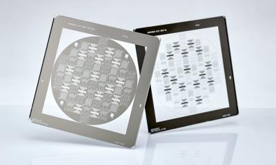
We also offer shared manufacturing services, or MultiProjectWafer (MPW) runs. Customers can access the different process flows that exist within our foundry and book some capacity to fabricate a few copies of a custom device; the cost of the run is diluted between the different customers accessing the MPW run, lowering the entry barrier for custom graphene devices. Within our GFAB services, the full suite of manufacturing capabilities enable fully customized devices, integrated at the back end of line (BEOL). Our different process flows, spanning different metallization and encapsulation schemes, enable many device architectures and pave the way for many real life applications in the field of sensing and optoelectronics.

In all of the devices manufactured within our foundry (from our standard GFETs to the custom designs for our customers), we guarantee an average mobility >1000 cm2/V·s with a guaranteed yield of 75%.
This represents an excellent platform for rapid device prototyping, pilot production or even larger volume demands. The users are able to dramatically accelerate the development of their device/applications, removing the burden of fabrication and allowing them to focus on development, data acquisition and analysis. Having a reliable, consistent source of graphene-based devices is one of the cornerstones for this material to be put into products and be ubiquitous in everyday's devices.