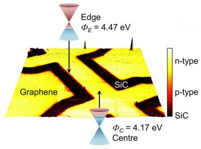
Researchers from the UK's National Physical Laboratory (BPL) discovered that graphene conductivity in the edges is different compared to the center of the material.

Using local scanning electrical methods, the researchers examined the local nanoscale properties of a graphene Hall bar device. It turns out that at the center of the channel, the graphene is n-doped (electron conduction) while at the edges it is p-doped (hole conduction).
The smaller the graphene is, the more these properties change. In a very small graphene, the altered properties may affect up to 25% of the material.
The researchers note that this inversion effect was stronger after cleaning the graphene - which leads them to believe that the change at the edges is caused by defects at the channel edge introduced by the plasma etching process.