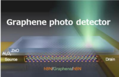
NTT Corporation and the National Institute for Materials Science (NIMS) have jointly reported the realization of what they define as "the world's fastest zero-bias operation (220 GHz) of a graphene photodetector (PD)". The research conducted by NTT and NIMS has also, according to the statement, clarified the optical-to-electrical (O-E) conversion process in graphene for the first time.
Graphene is a promising photodetection material for enabling high-speed O-E conversion at wavelength ranges where existing semiconductor devices cannot operate, thanks to its high sensitivity and high-speed electrical response to a wide range of electromagnetic waves, from terahertz (THz) to ultraviolet (UV). However, until now, the demonstrated zero-bias operating speed has been limited to 70 GHz due to conventional device structure and measurement equipment. For this reason, the challenge for graphene PDs is to demonstrate 200-GHz operation speeds and clarify graphene's inherent properties, such the process of optical-to-electrical conversion.
In their study, NTT and NIMS demonstrated high-speed operation with a 3dB bandwidth of 220 GHz by removing the current delay caused by the device structure by using zinc oxide (ZnO) thin film as the gate material and by using on-chip THz spectroscopy technology to read out the current at high speed. The research also found a trade-off between operating speed and sensitivity by comparing the characteristics of PDs fabricated with graphene of different qualities. The findings could enable graphene PDs to be optimized according to their intended use, such as in optical sensors prioritizing sensitivity or O-E signal converters prioritizing speed.
The research group studied O-E conversion in graphene, focusing on the photothermoelectric (PTE) effect, which enables zero-bias operation required to improve power consumption and the signal-to-noise ratio. Furthermore, the research showed that, contrary to conventional understanding, the response time of the current is almost independent of the size of the PD. Moreover, the time from light irradiation to current generation can be varied significantly from less than 100 fs to more than 4 ps, depending on the carrier density.
These results demonstrate the potential of graphene as a high-speed broadband PD. However, the graphene in this experiment was exfoliated from graphite, making it unsuitable for mass production. In the future, NTT researchers will evaluate PDs using large-area graphene that can be mass-produced. Researchers have actively been creating materials that do not exist in nature by layering graphene and other two-dimensional materials (single or multi-layered atomic layer materials). Researchers will also search for materials that can achieve even faster operation by making the most of this technology. You can read the full details about this innovation here.
