March 2011

GSAS to host a session on Graphene in Grenoble France

The global school for advance studies (GSAS) will host a session on Graphene on June 21-22 in the GIANT Innovation Campus in Grenoble, France. This session will create several teams of young researchers and challenge them to design a team project that will leverage their complementary strengths. Each team will have members from around the world and a balanced range of capabilities including materials synthesis, characterization, device design and fabrication, theory and measurement, etc.

The teams will receive project mentoring from leading graphene experts including Harry Kroto and Sumio Iijima. The most promising project will be implemented at CEA Laboratories on the GIANT innovation campus in January, 2012
Read the full story Posted: Mar 30,2011

Silicene - a new atom-thin honeycomb material made from Silicon atoms

Phyisicists created atom-thin sheets of silicon - and named the new material Silicene. The idea to create such sheets from Silicon emerged in 2007 - even though silicon doesn't naturally form the required atomic bonds. Silicene has a similar pattern to Graphene and possibly has the same electronic properties and might have advantages of Graphene because silicon is more integrateable into today's electronic devices.

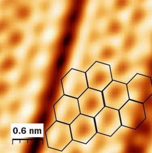
The Silicene was created by growing a thin layer of silicon on top of a ceramic material called zirconium diboride. X-rays shined on this thin layer of silicon revealed a honeycomb of hexagons similar to the structure of graphene.

Read the full story Posted: Mar 25,2011

Scientist predicts that Graphene will skip FET and jump straight to quantum devices

Georgia Tech Professor Walt de Heer predicts that Graphene will not follow the model of using standard field-effect transistors, but will pursue devices that use ballistic conductors and quantum interference. The Professor's research team hopes to show a basic quantum interference switch within a year.

Taking advantage of the wave properties will allow electrons to be manipulated with techniques similar to optical control, for instance switching may be carried out using interference - separating beams of electrons and then recombining them in or out of phase to switch the signal.

Read the full story Posted: Mar 24,2011

Graphene Quantum Dots can be made from Buckyballs

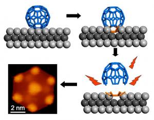
Researchers from Singapore discovered that graphene quantum dots can be made from carbon-60 molecules (C60, known as buckyballs). This is the first "bottom-up" approach to make graphene quantum dots - which could lead to more efficient and cheaper designs.

Graphene-based Quantum Dots photo

The QDs are smaller then 10nm in size and are all in the same size and shape. The idea is to decompose C60 molecules at high temperatures on a ruthenium metal surface. The metal acts as a catalyst and causes the C60 to break down into carbon clusters. The researchers were able to limit cluster aggregation and at around 825K temperature the clusters merged and crystallized into hexagonal-shaped graphene QDs.

Read the full story Posted: Mar 23,2011

Oxford Nanopore to commercialize Harvard's Graphene DNA Sequencing technology

Oxford Nanopore has reached an agreement with Harvard University to develop technology that uses graphene for DNA and RNA sequencing. This technology was developed in the Harvard laboratories of Professors Jene Golovchenko, Daniel Branton, and Charles Lieber and Oxford Nanopore now has exclusive rights to develop and commercialize it.

The Harvard team used graphene to separate two chambers containing ionic solutions, and created a hole - a nanopore in the graphene. The group demonstrated that the graphene nanopore could be used as a trans-electrode, measuring a current flowing through the nanopore between two chambers. The trans-electrode was used to measure variations in the current as a single molecule of DNA was passed through the nanopore. This resulted in a characteristic electrical signal that reflected the size and conformation of the DNA molecule.

Read the full story Posted: Mar 11,2011

TI demonstrates growing large-grain graphene crystals

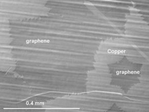
Texas Instruments (TI) is researching Graphene-growing for quite a while, and have recently demonstrated growing large-grain graphene crystals (up to 0.5 millimeter diameter) using low-pressure chemical vapor deposition inside copper-foil enclosures (and they are investigating growth on other substrates, more stable then copper). TI says that the new method allows them to grow graphene that is 30 times larger than before.

This research is conducted in collaboration with IBM's T.J. Watson Research Center, the Nanoelectronic Research Initiative (NRI), and the University of Texas.

Read the full story Posted: Mar 04,2011

Placing graphene on boron nitride could significantly improve its electronic properties

Researchers from the University of Arizona, MIT and Japan's NMSI discovered that placing graphene on boron nitride (instead of the commonly used silicon dioxide) could significantly improve its electronic properties.

Boron nitride is structurally basically the same as Graphene, but it's different electronically - Graphene is a conductor and boron nitride is an insulator. Putting graphene on an insulator makes it possible to study the properties of Graphene alone.

Read the full story Posted: Mar 02,2011