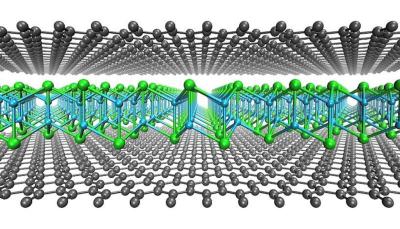
Researchers at the University of Vienna, in collaboration with the Universities of Tübingen, Antwerp and CY Cergy Paris and working with Danubia NanoTech, have developed a graphene-based method to produce 2D materials. They have already produced a new 2D material made of copper and iodine atoms sandwiched between two graphene sheets.
 A single layer of cuprous iodide encapsulated in between two sheets of graphene (gray atoms). Image from Phys.org, credit: Kimmo Mustonen, Christoph Hofer and Viera Skákalov
Following the 2D copper iodide, the researchers have already expanded the synthesis method to produce other new 2D materials. "The method seems to be truly universal, providing access to dozens of new 2D materials. These are truly exciting times," Kimmo Mustonen, the lead author of the study, said.
In the recent study, the researchers synthesized 2D cuprous iodide that was stabilized in a graphene sandwich, as the first example of a material that does not otherwise exist in normal laboratory conditions. The synthesis utilizes the large interlayer spacing of oxidized graphene multilayers, which allows iodine and copper atoms to diffuse into the gap and to grow the new material. The graphene layers here have an important role imposing a high pressure on the sandwiched material that thus becomes stabilized.
"As so often, when we first saw the new material in our microscopy images, it was a surprise", says Kimmo Mustonen. "It took us quite some time to figure out what the structure precisely was. This enabled us together with Danubia NanoTech company, headed by Viera Skákalová, to design a chemical process for producing it in large scale", he continues. Understanding the structure was a joint effort of scientists from the Universities of Vienna, Tübingen, Antwerp and CY Cergy Paris. "We had to use several electron microscopy techniques to make sure that we were really seeing a monolayer of copper and iodine and to extract the exact atom positions in 3D, including the latest methods we have recently developed", the second lead author Christoph Hofer adds.