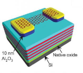
Researchers from Northwestern University are working on a new type of graphene-enhanced dielectric for semiconductors. A dielectric is an insulating layer that stabilizes the charge carriers in semiconductors, aiming to decrease the voltage that a transistor needs to function and make it more efficient.

Silicon dioxide is usually used as dielectric in semiconductors, but as electronics become smaller the SiO2 becomes thinner and less effective. The researchers aim to solve that problem by creating a dielectric with a greater ability to store charges, by developing a self-assembled nanodielectric (SAND) that is made up of layers of crosslinked organosilane molecules. The SAND works well with both organic and inorganic semiconductors and functions at a lower voltage than traditional dielectrics. That, plus the fact that they can be printed onto plastic surfaces, makes them especially suited for use in a variety of devices.
The researchers strive to commercialize their novel SAND and bring them from the lab to the real world through a startup company, Polyera, which offers a growing repertoire of advanced materials.