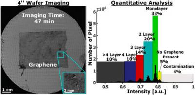
Spectroscopic Imaging Ellipsometry (SIE) is a powerful tool to characterize, analyze and investigate thicknesses, optical properties and defects or impurities of 2D-materials. Recently, researchers from the University of Cambridge, Accurion and the University of Applied Sciences and Arts in Gattingen Germany focused on ellipsometric contrast micrography (ECM), a fast intensity mode within spectroscopic imaging ellipsometry, and showed that it can be effectively used for noncontact, large area characterization of 2D materials like graphene to map coverage, layer number, defects and contamination.

The team has shown that imaging ellipsometry - in the mode of recording contrast micrographs - can be used to identify, test the quality and quantify 2D materials independently of the substrate and the material. Examples are graphene layers on Si with native oxide or directly on rough Cu catalyst foils as well as mono-layer hexagonal BN .

