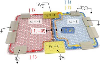
Researchers from France, South Korea, and Japan have created a graphene-based beam splitter for electronic currents. The tunable device’s operation is directly comparable to that of an optical interferometer. The team believes that the technology could enable electron interferometry to be used in nanotechnology and quantum computing. Quantum Hall valley splitter - schematic representation of the p â n junction. Image from article
An optical interferometer splits a beam of light in two, sending each beam along a different path before recombining the beams at a detector. The measured interference of the beams at the detector can be used to detect tiny differences in the lengths of the two paths. Recently, physicists have become interested in doing a similar thing with currents of electrons in solid-state devices, taking advantage of the fact that electrons behave similarly to waves in the quantum world.
The team’s interferometer design features a graphene p-n junction, which comprises a nanoscale flake of graphene where one side is p-doped and the other is n-doped by applying two different electric fields.
The device operates by first injecting an electron current at one corner of the n side, which causes two current loops to form on either side of the p-n boundary, flowing in opposite directions. While the edge of the p side carries a clockwise loop of spin-up electrons, the n side has two separate channels flowing anti-clockwise, each containing opposite electron spins.
At the point where the two loops first meet at the boundary, the effect of quantum tunneling means that a certain proportion of spin-up electrons on the n side will transfer to the p side. By applying a varying voltage to this point through a tunable gate, Roulleau and colleagues discovered that they could tightly control this tunneling fraction: an ability directly comparable to a tunable beam splitter used in optical interferometers.
At the other end of the boundary, the researchers then applied a second voltage to act as a reverse beam splitter, forcing electrons that had tunneled to recombine with the current on the n side. To determine the influence of these tunneling electrons, Roulleau’s team measured an output current on the p side, at the opposite corner to the current injection point.
In their observations, the team detected characteristic oscillations in this output current, which varied depending on the voltage and magnetic field strength applied to the first beam splitter. In analogy with the interference patterns seen in recombined interferometer beams, these oscillations indicated the phase differences between the recombined n side currents. The team will now aim to further compact their graphene flake design; potentially leading to new, highly advanced capabilities in both nanotechnology and quantum computing.