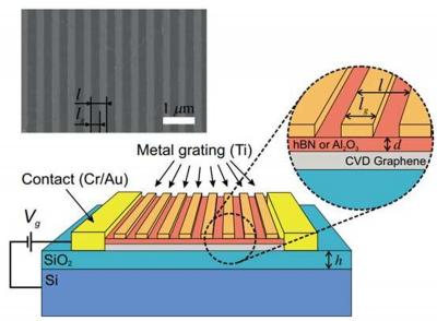
Researchers from the Moscow Institute of Physics and Technology (MIPT) and Valiev Institute of Physics and Technology in Russia have demonstrated resonant absorption of terahertz radiation in commercially available graphene. The team declared this to be an important step toward designing efficient terahertz detectors, which would enable faster internet and a safe replacement for X-ray body scans.
 Graphene-based transistor with a metal grating. Credit: Courtesy of the researchers
THz radiation, also known as T-waves, is considered difficult to generate and detect. This gave rise to the notion of a terahertz gap, which roughly refers to the 0.1-10 THz frequency band in the electromagnetic spectrum. There are no efficient devices for generating and detecting radiation in this range. Nevertheless, T-waves are very important for humanity: They do not harm the body and so could replace X-rays in medical scans. Also, T-waves could make Wi-Fi much faster and open the door to astronomical research that is thus far untapped .
Unfortunately, this phenomenon is not observed in a continuous sheet of a conductor illuminated with plane waves. The plasmon wavelength is too short compared with that of the photon, and so these two waves can hardly be synchronous. To address this issue, a metal grating is placed above the graphene film. It resembles a tiny comb with teeth less than a micrometer apart.
Dozens of techniques exist for producing graphene, which differ in terms of end product quality and labor intensity. Mechanical exfoliation yields extremely high-quality graphene. Unfortunately, graphene flakes manufactured by mechanical exfoliation are only micrometers across, take several months to produce, and end up too expensive for serial device design. CVD is an easier and more scalable alternative technique for graphene synthesis. The resulting graphene has poorer characteristics and more defects than the mechanically exfoliated one. But CVD is currently the technology best-suited for scaling up device production.
The Russian physicists set out to test whether such commercial-grade graphene is good enough for THz plasmon resonance excitation, which would make it a valid material for T-wave detectors.
Actually, a CVD-produced graphene film is not homogeneous. Like a polycrystal, it consists of numerous merged grains. Each one is an ordered region with a completely symmetrical atomic pattern. Grain boundaries, along with defects, make working with such graphene far from easy, study co-author and MIPT graduate student Elena Titova said.
It took the team over a year to master working with CVD graphene at the Institute’s Center of Shared Research Facilities. Meanwhile, the colleagues from the lab’s theoretical department were convinced that no plasmon resonance would be observed. The reason is that resonance visibility is determined by the so-called quality factor â that is, how many periods the field passes before the electron encounters a lattice defect. Theoretical estimates predicted a very low Q factor limited by frequent electron-defect collisions in CVD graphene. That said, the high electron mobility in graphene emerges not due to infrequent electron collisions, but due to a low mass of electrons, which enables their fast acceleration to a high velocity.
Despite the pessimistic theoretical predictions, the authors of the paper decided to still do the experiment. Their resolve was rewarded: The absorption spectra exhibited the peaks indicative of plasmon resonance in CVD-synthesized graphene.
The thing is that not all defects are the same, and electrons collide with different defects in direct current measurements and THz absorption measurements, comments the research supervisor, Dmitry Svintsov, who heads the MIPT Laboratory of 2D Materials for Optoelectronics. In a DC experiment, an electron will inevitably encounter grain boundaries on the way from one electrical contact to the other. But when exposed to T-waves, it will mostly fluctuate within a single grain, away from its boundaries. This means that defects impairing DC conductivity are actually ‘safe’ for T-wave detection.
A further mystery had to do with the frequency of resonant plasmon excitation, which disagreed with the previously existing theories. It turned out to be related to the geometry of the metal grating in an unexpected way. The team found that when positioned close to graphene, the grating modified the plasmon field distribution. This led to plasmon localization under the comb teeth, whose edges acted as mirrors for plasmons. The researchers formulated a very simple theory describing the phenomenon based on an analogy with the tight-binding model from solid-state physics. The theory reproduces the experimental data well without resorting to fitting parameters and can be used to optimize future T-wave detectors.