A group of scientists from the National Research University of Electronic Technology MIET (Russia), Technological Center AIMEN (Spain) and Forschungszentrum Jülich (Germany) has developed an approach for graphene physical and chemical modification avoiding the step of resist deposition, that can be useful for graphene-based electronics technologies.
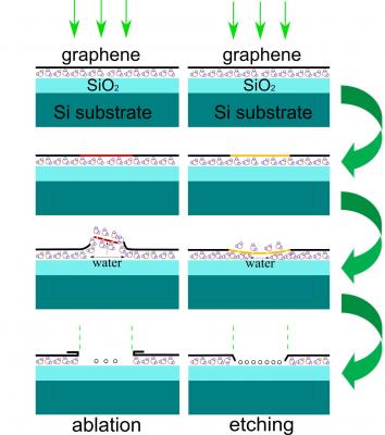
This work demonstrates the mask-less and resist-free patterning of graphene by two different routes: thermal ablation or oxidative etching. That means that by varying the parameters of laser pulses, chemical tuning (energy gap control) and isolation line patterning is possible in a single process without any chemicals. The same group published the results of graphene oxide reduction by using thermal and chemical effects from laser irradiation. Moreover the laser pulses provide 3D embossing of graphene that open the way for single processing of NEMS and microfluidic-based sensors in graphene.
The researchers explored the use of focused laser beam for graphene processing. They discovered the photochemical and physical effect on graphene can be separated under femtosecond laser pulsed irradiation. That means the possibility to separate the chemical reactions induced in graphene from thermal effects by using high energy laser pulses.
The technology is based on high-energy photons from UV lamps or focused femtosecond laser pulses. Depending on the initial state of the graphene and light source parameters, the process provides cleaning, etching, doping, oxidation, reduction and 3D modification of materials and patterning for different applications in electronics, biology and optics.

