Researchers succeed in synthesizing graphyne

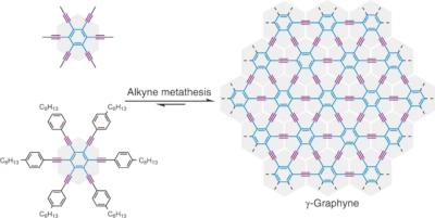
Researchers at the University of Colorado Boulder and Qingdao University of Science and Technology have managed to synthesize an illusive form of carbon called graphyne. Graphyne has long been of interest to scientists because of its similarities to graphene. However, despite decades of work and theorizing, only a few fragments have ever been created before now.

Graphyne created for first time image

"The whole audience, the whole field, is really excited that this long-standing problem, or this imaginary material, is finally getting realized," said Yiming Hu, lead author on the paper.

Read the full story Posted: May 22,2022

Japan launches a $8.5 million project to study 2.5D materials

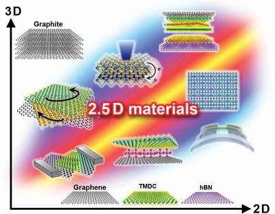
Japan's Ministry of Education, Culture, Sports, Science and Technology has launched a collaborative project to develop 2.5D materials. The project, titled "Science of 2.5 Dimensional Materials: Paradigm Shift of Materials Science Toward Future Social Innovation" includes 40 researchers in Japan, led by Prof. Ago Hiroki at Kyushu University.

2.5D material chart, Kyushu University

2.5D materials are made by stacking different 2D materials artificially by using advanced transfer techniques. These new materials are not limited by lattice constant or composition, and it is possible to control the material layers, and their stacking angle. These new materials could unlock new breakthroughs in materials science.

Read the full story Posted: May 07,2022

Researchers succeed in synthesizing single layers of hexagonal boron nitride on graphene

A research team led by the University of Michigan has developed a reliable, scalable method for growing single layers of hexagonal boron nitride on graphene.

Graphene-hBN structures can power LEDs that generate deep-UV light, which is impossible in today's LEDs, said Zetian Mi, U-M professor of electrical engineering and computer science and a corresponding author of the study. Deep-UV LEDs could drive smaller size and greater efficiency in a variety of devices including lasers and air purifiers.

Read the full story Posted: Apr 24,2022

Researchers detect evidence of strong electron correlation in a trilayer graphene/hBN moiré superlattice

Researchers from MIT, Harvard University, University of California at Berkeley, Lawrence Berkeley National Laboratory, China's Shanghai Jiao Tong and Fudan Universities and Japan's National Institute for Materials Science have taken a significant step toward understanding electron correlations.

In their new study, the researchers revealed direct evidence of electron correlations in a two-dimensional material called ABC trilayer graphene. This material has previously been shown to switch from a metal to an insulator to a superconductor.


Read the full story Posted: Mar 22,2022

MIT researchers manage to create a 2D polymer material for the first time

Researchers from MIT created a new 2D material, called 2DPA-1, which is the world's first 2D polymer. Until now, it was actually believed to be impossible to induce polymers into a 2D sheet.

To create the material, the researchers used a novel polymerization process, that was used to generate a two-dimensional sheet called a polyaramide. For the monomer building blocks of the material, they use a compound called melamine, which contains a ring of carbon and nitrogen atoms. Under the right conditions, these monomers can grow in two dimensions, forming disks. These disks stack on top of each other, held together by hydrogen bonds between the layers, which make the structure very stable and strong.

Read the full story Posted: Feb 05,2022

Graphene enables the creation of new 2D materials

Researchers at the University of Vienna, in collaboration with the Universities of Tübingen, Antwerp and CY Cergy Paris and working with Danubia NanoTech, have developed a graphene-based method to produce 2D materials. They have already produced a new 2D material made of copper and iodine atoms sandwiched between two graphene sheets.
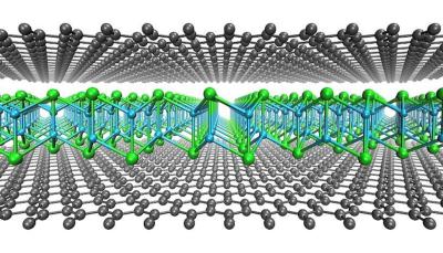
A single layer of cuprous iodide encapsulated in between two sheets of graphene imageA single layer of cuprous iodide encapsulated in between two sheets of graphene (gray atoms). Image from Phys.org, credit: Kimmo Mustonen, Christoph Hofer and Viera Skákalov

Following the 2D copper iodide, the researchers have already expanded the synthesis method to produce other new 2D materials. "The method seems to be truly universal, providing access to dozens of new 2D materials. These are truly exciting times," Kimmo Mustonen, the lead author of the study, said.
Read the full story Posted: Jan 21,2022

Researchers demonstrate how graphene can improve perovskite solar cells

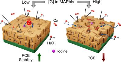
Recent research has shown that the incorporation of graphene-related materials improves the performance and stability of perovskite solar cells. Graphene is hydrophobic, which can enhance several properties of perovskite solar cells. Firstly, it can enhance stability and the passivation of electron traps at the perovskite’s crystalline domain interfaces. Graphene can also provide better energy level alignment, leading to more efficient devices.

Improving Solar Cells with Pristine Graphene on Lead Iodide Films image

In a recent study, Spain-based scientists used pristine graphene to improve the properties of MAPbI3, a popular perovskite material. Pristine graphene was combined with the metal halide perovskite to form the active layer of the solar cells. By analyzing the resulting graphene/perovskite material, it was observed that an average efficiency value of 15% under high-stress conditions was achieved when the optimal amount of graphene was used.

Read the full story Posted: Nov 25,2021

Researchers develop ultra-efficient 'clean' technique to control the properties of graphene

Researchers from Columbia University and collaborators from Korea's Sungkyunkwan University and Japan's National Institute for Materials Science have reported that graphene can be efficiently doped using a monolayer of tungsten oxyselenide (TOS) that is created by oxidizing a monolayer of tungsten diselenide.

The new results relied on a cleaner technique to manipulate the flow of electricity, giving graphene greater conductivity than metals such as copper and gold, and raising its potential for use in telecommunications systems and quantum computers.

Read the full story Posted: Nov 02,2021

Twisted bi-layer graphene displays unique quantum behavior

Scientists studying two different configurations of bilayer graphene have detected electronic and optical interlayer resonances. In these resonant states, electrons bounce back and forth between the two atomic planes in the 2-D interface at the same frequency. By characterizing these states, they found that twisting one of the graphene layers by 30 degrees relative to the other, instead of stacking the layers directly on top of each other, shifts the resonance to a lower energy. From this result they deduced that the distance between the two layers increased significantly in the twisted configuration, compared to the stacked one. When this distance changes, so do the interlayer interactions, influencing how electrons move in the bilayer system. An understanding of this electron motion could inform the design of future quantum technologies for more powerful computing and more secure communication.

Today’s computer chips are based on our knowledge of how electrons move in semiconductors, specifically silicon, said first and co-corresponding author Zhongwei Dai, a postdoc in the Interface Science and Catalysis Group at the Center for Functional Nanomaterials (CFN) at the U.S. Department of Energy (DOE)’s Brookhaven National Laboratory. But the physical properties of silicon are reaching a physical limit in terms of how small transistors can be made and how many can fit on a chip. If we can understand how electrons move at the small scale of a few nanometers in the reduced dimensions of 2-D materials, we may be able to unlock another way to utilize electrons for quantum information science.

Read the full story Posted: Aug 26,2021