New model describes geometric features of carbon networks and their influence on the material's properties

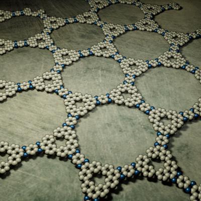
Scientists at Tohoku University and colleagues in Japan have developed a mathematical model that abstracts the key effects of changes to the geometries of carbon material and predicts its unique properties.

Geometric model of 3D curved graphene with chemical dopants image

Scientists generally use mathematical models to predict the properties that might emerge when a material is changed in certain ways. Changing the geometry of three-dimensional (3D) graphene, which is made of networks of carbon atoms, by adding chemicals or introducing topological defects, can improve its catalytic properties, for example. But it has been difficult for scientists to understand why this happens exactly.

Read the full story Posted: Jul 19,2021

Researchers develop a new method for quick and efficient synthesis of nanographenes

A research team at Nagoya University in Japan has developed a new technique for synthesizing nanographenes, remarkable materials with a vast number of potential structures that can even exhibit electric and magnetic characteristics beyond those of graphene.

Since each nanographene exhibits different physical characteristics, the key to applied nanographene study is to determine the relationship between the structure and characteristics of as many nanographenes as possible.

Read the full story Posted: Jun 30,2021

Gnanomat announced new commercially available Graphene-Silver nanocomposite

Gnanomat recently announced the launch of its new commercially-available graphene-based nanocomposite.

A new Graphene-Silver nanocomposite commercially available by Gnanomat image

Graphene Silver nanocomposite, a product supplied as a dry powder, is made of pristine graphene coated with silver nanoparticles. This type of material has been shown to have great potential in scientific literature, in applications such as inks on textiles for highly conductive wearable electronics, electrochemical sensors, catalyst, antibacterial activity and detection of heavy metal ions.

Read the full story Posted: Feb 25,2021

Researchers examine 'Kagome' graphene and report promising results

Researchers from the Department of Physics and the Swiss Nanoscience Institute at the University of Basel, working in collaboration with the University of Bern, have recently produced and studied a compound referred to as "kagome graphene", that consists of a regular pattern of hexagons and equilateral triangles that surround one another. The name kagome comes from the old Japanese art of kagome weaving, in which baskets are woven in the same pattern.

Kagome graphene revealed to have fascinating properties imageKagome graphene is characterized by a regular lattice of hexagons and triangles. Credit: R. Pawlak, Department of Physics, University of Basel

The team's measurements have reportedly delivered promising results that point to unusual electrical or magnetic properties of the material.

Read the full story Posted: Feb 16,2021

New technique may enable large-area integration of 2D materials

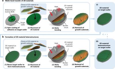
Researchers affiliated with the Graphene Flagship from RWTH Aachen University, Universität der Bundeswehr München and AMO in Germany, KTH Royal Institute of Technology in Sweden and with Protemics have reported a new method to integrate graphene and 2D materials into semiconductor manufacturing lines, a milestone for the recently launched 2D-EPL project.

Schematic illustration of the methodology for wafer-level transfer of two-dimensional materials imageImage from Nature Communications

Two-dimensional (2D) materials have a huge potential for providing devices with much smaller size and extended functionalities with respect to what can be achieved with today's silicon technologies. But to exploit this potential, it is vital to be able to integrate 2D materials into semiconductor manufacturing lines - a notoriously difficult step. This new technique could be a step in the right direction as far as solving this problem is concerned.

Read the full story Posted: Feb 15,2021

Researchers develop monolayer graphene-based reversible self-folding structures

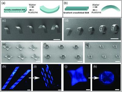
A team of scientists at Johns Hopkins University in the U.S. has designed a mass-production strategy to create monolayer graphene-based reversible self-folding structures. The material may find potential uses in microfluidics and micromechanical systems.

 Share  Email  Home Nanotechnology Nanophysics Home Nanotechnology Nanomaterials JANUARY 11, 2021 FEATURE  Self‐folding 3-D photosensitive graphene architectures imageMechanism and versatility of self‐folding SU8 films. Image from article

As proof of concept, the team achieved complex and functional devices in the form of rings, polyhedra, flowers and origami birds. They then integrated gold electrodes to the constructs to improve their detection sensitivity. The experiments suggest a comprehensive framework to rationally design and fabricate scalable and complex, 3D, self-folding optical and electronic devices by folding 2D monolayer graphene.

Read the full story Posted: Jan 12,2021

University of Washington team finds that carefully constructed stacks of graphene can exhibit highly correlated electron properties

A research team led by the University of Washington recently reported that carefully constructed stacks of graphene can exhibit highly correlated electron properties. The team also found evidence that this type of collective behavior likely relates to the emergence of exotic magnetic states.

We’ve created an experimental setup that allows us to manipulate electrons in the graphene layers in a number of exciting new ways, said co-senior author Matthew Yankowitz, a UW assistant professor of physics and of materials science and engineering. Yankowitz led the team with co-senior author Xiaodong Xu, a UW professor of physics and of materials science and engineering.

Read the full story Posted: Oct 07,2020

Chalmers team designs method for fabricating atomically sharp nanostructures

Researchers at Chalmers University in Sweden have recently reported a facile and controllable anisotropic wet etching method that allows scalable fabrication of transition metal dichalcogenides (TMD) metamaterials with atomic precision. The team says that this new method has great potential for various layered structures like MoS2 and WS2 and graphene.

Etching hexagonal nanostructures in TMD materials imageProcess of etching hexagonal nanostructures in TMD materials. Image from article

They showed that materials can be etched along certain crystallographic axes, such that the obtained edges are nearly atomically sharp and exclusively zigzag-terminated. This results in hexagonal nanostructures of predefined order and complexity, including few-nanometer-thin nanoribbons and nanojunctions. Thus, this method enables future studies of a broad range of metamaterials through atomically precise control of the structure.

Read the full story Posted: Oct 06,2020

First Graphene to collaborate with M&I Materials on development of graphene-enhanced products

Graphene raw materials supplier First Graphene and UK-based specialist materials manufacturer M&I Materials have agreed to collaborate to develop an extended range of graphene-enhanced products.

Both companies are partners at Manchester’s Graphene Engineering and Innovation Centre (GEIC), a facility dedicated to the commercialization of graphene. The GEIC has played a big part in enabling this collaboration and has benefited both parties in terms of the close working relationship at the same location and the extensive facilities and support available on site.

Read the full story Posted: Oct 06,2020

Cooling graphene causes buckling that could further the search for quantum materials

Graphene buckles when cooled while attached to a flat surface, resulting in patterns that could benefit the search for novel quantum materials and superconductors, according to a recent Rutgers-led research.

Quantum materials host strongly interacting electrons with special properties, such as entangled trajectories, that could provide building blocks for super-fast quantum computers. They also can become superconductors that could slash energy consumption by making power transmission and electronic devices more efficient.

Read the full story Posted: Aug 13,2020