October 2010

Korean researchers use Grapene to make LEDs

Korean researchers from the Seoul National University say that they've developed a technology to produce LEDs by using Graphene sheets. They have cultured nitride thin-films on a sheet on Graphene. The nitride thin films show excellent characteristics at room temperature, such as stimulated emission.

Read the full story Posted: Oct 31,2010

Graphene nanoflakes can be used for water desalination

Researchers from Australia and Shanghai have developed a Capacitive deionization (CDI) application that uses graphene-like nanoflakes as electrodes for capacitive deionization. Capacitive deionization (CDI) is a relatively new way to purify water. It is cost effective and energy efficient. The team believes that Graphene can be an excellent candidate for the electrode material for the CDI. This is not the first time we hear about Graphene being used to clear drinking water...

The basic concept behind CDI is to force charged ions toward oppositely polarized electrodes through imposing a direct electric field: brackish water flows between pairs of high surface area carbon electrodes that are held at a potential difference of about 1-2 volts. The ions and other charged particles, such as microorganisms, are attracted to and held on the electrode of opposite charge. The negative electrode attracts positively charged ions (cations) such as calcium, magnesium and sodium, while the positively charged electrode attracts negative ions (anions) such as chloride, nitrate, and silica (read more about how CDI technology works here).

Read the full story Posted: Oct 27,2010

Researchers use water to open and tune Graphene's band gap

Researchers from the Rensselaer Polytechnic Institute has developed a new method to open and tune the band gap of Graphene - using water. By exposing the Graphene film to humidity, the researchers created the band gap. A band gap is required to create transistors, so this can help pave the way for Graphene transistors.

The researchers found out that by changing the amount of water absorbed on one side of the Graphene film, they can tune the band gap to any value from 0 to 0.2 electron volts, and this is reversible under vacuum.

Read the full story Posted: Oct 26,2010

Researchers: Mass can be created inside Graphene

Abdulaziz Alhaidari from the Saudi Center for Theoretical Physics in Saudi Arabia claim that if you reduce the number of space-like dimensions in graphene from two to one, the mass-less equations that describe the behavior of electrons and holes will change to include a term for mass. In effect, compactifying dimensions creates mass.

Graphene mass generation image

The idea is that you roll the Graphene up, and This changes the sheet into a tube that is effectively 1-dimensional, at least as far as the electrons and holes are concerned.

Read the full story Posted: Oct 21,2010

Researchers develop a flexible Graphene-based Memristor

Researchers from ETRI, South Korea has recently build a flexible Memristor using thin Graphene oxide films. These new Memristors should be cheaper and easier to make as they can be roll-to-roll printed on plastic sheets.

Memristors change their resistance depending on the direction and amount of voltage applied, and they remember this resistance when the voltage is removed. The researchers use a similar design to the one used by HP (which hopes to have Memristor chips ready within 3 years), but they are swapping the titanium dioxide that HP is using with Graphene Oxide. This makes them cheap and flexible, but also much larger (1000 times in fact!). So this is not suited for high-density memory, but rather for applications such as RFID for example. 

Read the full story Posted: Oct 14,2010

Tunneling-spin-injection achieved in graphene, could enable graphene-based Spintronics

Researchers from the University of California, Riverside successfully achieved tunneling-spin-injection into Graphene. The researchers inserted a nanometer-thick insulating layer, known as a tunnel barrier, in between the ferromagnetic electrode and the graphene layer. They found that the spin injection efficiency increased dramatically. A 30-fold increase, actually. This could lead to graphene-based Spintronic devices.

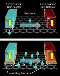
The team also made an unexpected discovery that explains short spin lifetimes of electrons in graphene that have been reported by other experimental researchers. People usually assume that the Hanle measurement accurately measures the spin lifetime, but this result shows that it severely underestimates the spin lifetime when the ferromagnet is touching the graphene, said Wei Han, the first author of the research paper and a graduate student. This is good news because it means the true spin lifetime in graphene must be longer than reported previously potentially a lot longer.

Read the full story Posted: Oct 14,2010

Researchers develop the first triple-mode graphene amplifier

Researchers from Rice University and the University of California, Riverside (UCR) has demonstrated the first triple-mode graphene amplifier. By leveraging the ambipolarity of charge transport in graphene, the amplifier can be configured in the common-source, common-drain, or frequency multiplication mode of operation by changing the gate bias. This is the first demonstration of a single-transistor amplifier that can be tuned between different modes of operation using a single three-terminal transistor.

Read the full story Posted: Oct 12,2010

Angstron introduces new high-quality graphene oxide product

Angstron Materials introduced a new high quality graphene oxide product, available in 0.5% water or solvent dispersion. The new graphene oxide product is available in large quantities and Angstron provides next-day delivery. The material is only 0.34 1.0 nanometers thick and is nearly transparent at visible light wave making the material especially suited to applications for transparent coatings.

Read the full story Posted: Oct 10,2010

New "templated growth" technique to make Graphene

Researchers at the Georgia Institute of Technology have developed a new way to make Graphene using a "templated growth technique. The technique involves etching patterns into the silicon carbide surfaces on which epitaxial graphene is grown. The patterns serve as templates directing the growth of graphene structures, allowing the formation of nanoribbons of specific widths without the use of e-beams or other destructive cutting techniques. Graphene nanoribbons produced with these templates have smooth edges that avoid electron-scattering problems.

The new technique has been used to fabricate an array of 10,000 top-gated graphene transistors on a 0.24 square centimeter chip believed to be the largest density of graphene devices reported so far.

Read the full story Posted: Oct 06,2010