Graphene used to build the world's smallest FM transmitter

Researchers from Columbia University used graphene to produce the world's smallest FM radio transmitter using NEMS (nanoelectromechanical system, a scaled-down versions of MEMS which are used mostly for sensing of vibration or acceleration). This is not a practical FM radio design, but this technology may be used in wireless signal processing.

The researchers built a voltage controlled oscillator (VCO) that is used to create a FM signal. They used graphene to make a NEMS device with a frequency of about 100 Mhz (FM radio uses 87.7 to 108 Mhz). Low-frequency music signals from an iPhone were used to module the carrier signal, and these can be heard by using an ordinary FM receiver.
Read the full story Posted: Nov 19,2013

Archer Exploration and the University of Adelaide produced graphene products from medium-grade graphite

Archer Exploration, in collaboration with the University of Adelaide, has produced a wide number of graphene and intercalated graphite products from raw graphite, and from Campoona (Australia) medium-grade graphite concentrates.

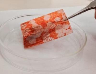
Archer announced that University researchers managed to produce graphene oxide sheets, nanosheets, membranes, powders, films, and electrodes. Archers aims to produce high grade to ultra-pure natural flake graphite and manufacture high tech, high-value graphene products.

Read the full story Posted: Nov 19,2013

Placing graphene on boron-nitride opens a bandgap, but only at a certain angle

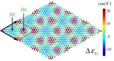
Researchers from the University of Twente have looked into graphene's behavior when it is placed on boron nitride. It turns out that if the graphene is placed in a certain angle over the BN, it opens a bandgap. If it is placed in a random angle, the band gap will not open.

The researchers also discovered that if the graphene/BN structure is placed on copper, that can be contacted with other devices, a charge distribution (dipole layer) is also formed on the interface between copper and boron nitride.

Read the full story Posted: Nov 19,2013

Applied Graphene Materials to go public tomorrow in the UK

Last month we reported that UK's Applied Graphene Materials (AGM, previously Durham Graphene Science) plan to raise £10 million by going public in the UK's AIM stock exchange. Today it is reported that AGM's offering will go live tomorrow (November 20).

The company will offer 7.09 million shares at 155 pence each. Following the placement, AGM will have 16.8 million shares, and the market capitalization will be £26.2 million (a little over $42. million).

Read the full story Posted: Nov 19,2013

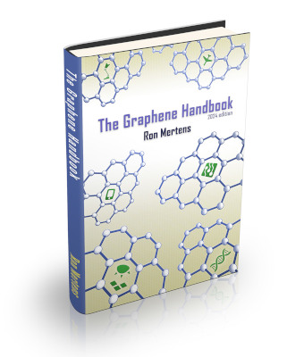
Introducing The Graphene Handbook

Today I'm happy and excited to announced my new book, released today - The Graphene Handbook. The Graphene Handbook is a comprehensive guide to graphene technology, industry and market.

Reading this book, you'll learn all about:

  • The properties of graphene
  • Different production methods
  • Possible graphene applications
  • The latest graphene research
  • The current market for graphene materials and products
  • The main graphene challenges
  • Other promising 2D materials

The book also provides:

  • A history of graphene developments
  • A graphene investment guide
  • A comprehensive list of graphene companies
  • A guide to other carbon allotropes

The Graphene Handbook costs $97 for the digital (PDF) edition or $149.99 for the printed edition. We also offer site and enterprise licenses, and academic discounts. If you're interested, click here for more information (including a table of contents).

Read the full story Posted: Nov 18,2013

Graphene successfully grown on single-crystal silver substrate

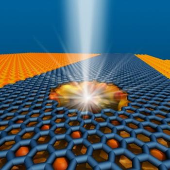
Researchers from Northwestern University and Argonne National Laboratory demonstrating the first growth of graphene on a single-crystal silver substrate. This method could be used to advance graphene-based optical devices (as silver is a widely used material to enhance optical properties) and enable the interfacing of graphene with other two-dimensional materials.

Silver substrates are chemically inert and have a relatively low melting point, which means it is difficult to use CVD technologies. The researchers used a graphite carbon source and deposited atomic carbon (rather than a carbon-based molecular precursor) onto the silver substrate. This allowed them to use low temperature and this process does not need a chemically active surface.

Read the full story Posted: Nov 16,2013

UT Austin researchers grow large graphene crystals with exceptional electrical properties

Researchers from The University of Texas at Austin (UT Austin) used surface oxygen to grow centimeter-size single graphene crystals on copper. These are very large single crystals, that feature exceptional electrical properties, are about 10,000 times as large as the largest crystals made at the University only four years ago.

The researcher explain that they are controlling the growth of tiny graphene nuclei, and using Oxygen at the right surface concentration means only a few nuclei grow, and winners can grow into very large crystals. By increasing the single-crystal domain sizes, the electronic transport properties will be dramatically improved and lead to new applications in flexible electronics.

Read the full story Posted: Nov 15,2013

UPenn established a new research center to developer layered materials

Penn State University (UPenn) and the Materials Research Institute have launched a center to research 2D materials. Specifically, the center aims to discover new 3D materials made by stacking 2D materials. They say that 2D materials could be used to make new hybrid 3D layered structures with a wide range of applications not yet imagined.

A dozen Penn State faculty members are involved in the center, including theorists, materials chemists, experimental physicists and experts in 2D synthesis.

Read the full story Posted: Nov 15,2013

UPenn researchers increase graphene-based DNA sequencing speed dramatically

Researchers from the University of Pennsylvania developed a new sensitive DNA sensor (sequencer) made from graphene drilled with nanopores. The same team already developed such a sensor in 2010, but this new method increases sequencing speed dramatically.

The idea is that the researchers have now measured current directly from the graphene, whereas before they measured ionic current in the solution as it goes through the pore. The researchers use graphene nanoribbons (GNRs), and when they pass a DNA base through the material, it modules the electrical current - in a different way for each base. The current in this method is a thousand times higher than in the previous method, which means measurements can be done a thousand times faster.

Read the full story Posted: Nov 15,2013

Only one week left to enjoy the 34% launch discount on the Graphene Patent Newsletter

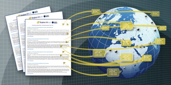
Three weeks ago we launched the Graphene Patent Newsletter, a daily newsletter that provides graphene patents updates from over 85 patent offices worldwide. When we launched, we offered a special launch discount: $100 off the normal yearly subscription rate ($300). This discount is only valid until November 21st, so here's your last chance to enjoy this discount. If you haven't done so yet, contact us now to activate your free 2-week trial or order your subscription!

The Graphene Patent newsletter at a glance:

  • A subscription-based news service (daily)
  • Provides patent applications, grants and expiration monitoring from over 85 countries (including the US, EU, China, Japan and Korea)
  • This manually-edited service is brought to you by two trustworthy companies
  • The best and easiest way to monitor global graphene patents!
  • A must-have tool for academic researchers and graphene companies!

Read the full story Posted: Nov 15,2013