Scientists at Columbia University made use of graphene and boron nitride to create a suitable environment in which to study other 2D semiconductors: Two layers of boron nitride are used to keep the environment away from the material under test, while graphene provides electrical connections.
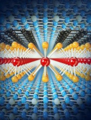
This method may be suitable for testing all 2D materials. The combination of BN and graphene electrodes cam be compared to a socket into which it is possible to place many other materials and study them in an extremely clean environment to understand their true properties and potential.
Source: electronicsweekly
Posted: Apr 29,2015 by Roni Peleg