Graphene Semiconductors: Introduction and Market status
What are semiconductors?
A semiconductor is a material (commonly a solid chemical element or compound) with distinct electrical properties: in some cases it will conduct electricity, but not in others. Thus, control of electrical current is enabled. A semiconductor's conductance varies depending on the current or voltage applied to a control electrode, or on the intensity of irradiation by infrared (IR), visible light, ultraviolet (UV), or X rays.

Semiconductors can be found at the heart of modern electronics. Some examples include microprocessor chips and transistors, and virtually any device that is computerized or uses radio waves relies on semiconductors. Nowadays, the most commercially important semiconductor is silicon, although many others are also in use.
What is graphene?
Graphene is a one-atom-thick layer of carbon atoms arranged in a hexagonal lattice. It is the building-block of Graphite (which is used, among others things, in pencil tips), but graphene is a remarkable substance on its own - with a multitude of astonishing properties which repeatedly earn it the title "wonder material".
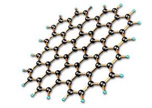
Graphene is the thinnest material known to man at one atom thick, and also incredibly strong - about 200 times stronger than steel. On top of that, graphene is an excellent conductor of heat and electricity and has interesting light absorption abilities. Graphene has potential to revolutionize many applications, among these are solar cells, batteries, sensors and more.


Graphene as a semiconductor
Semiconductors are defined by their band gap: the energy required to excite an electron stuck in the valence band, where it cannot conduct electricity, to the conduction band, where it can. The band gap needs to be large enough so that there is a clear contrast between a transistor's on and off states, and so that it can process information without generating errors.
Among graphene's superlative properties is exceptional electrical conductivity. This property makes the material attractive for many applications, but it is problematic for use as a semiconductor. For that, graphene would need a bandgap (which it normally lacks), or in other words to behave not just as a conductor but to also have an insulator mode.
Scientists have found various methods to introduce a bandgap to graphene. By fabricating graphene in specific shapes (like ribbons), by using certain growth methods paired with specific materials, by using graphene's morphological structure (namely wrinkles), by doping the material and more. Other 2D materials can be used instead or together with graphene, that have an inherent bandgap. These materials may prove to be an easier path towards next-gen semiconductor based devices.
Researchers succeed in creating graphene-based functional semiconductor
Researchers at the Georgia Institute of Technology and China's Tianjin University have created a novel functional semiconductor made from graphene, potentially opening the door to various next-gen electronics.
This discovery comes at a time when silicon, the material from which nearly all modern electronics are made, is reaching its limit in the face of increasingly faster computing and smaller electronic devices. The semiconductor made from graphene is compatible with conventional microelectronics processing methods – a necessity for any viable alternative to silicon.
The European Commission announces a €20 million investment in a new plant for graphene electronics
The European Commission (EC) has announced a â¬20 million investment in the next generation of electronics and semiconductors. The 2D Experimental Pilot Line (2D-EPL) was officially launched as the first graphene foundry to integrate graphene and layered materials into semiconductor platforms. The new project aims to keep Europe at the forefront of this technological revolution.
Born within the EU-funded project, the Graphene Flagship, the 2D-EPL will cover the entire value chain, from tool producers and chemical and material providers to manufacturing lines. This collaborative project will integrate several Graphene Flagship members to pioneer the fabrication of new prototype electronics, photonic devices and sensors integrating graphene and layered materials.
Researchers manage to grow GNRs directly on top of silicon wafers
Scientist from the University of Wisconsin-Madison are working towards making more powerful computers a reality. To that end, they have devised a method to grow tiny ribbons of graphene directly on top of silicon wafers. Graphene ribbons have a special advantage over graphene sheets - they become excellent semiconductors.
 Graphene nanoribbons on silicon wafers could help lead the way toward super fast computer chips. Image courtesy of Mike Arnold
Compared to current technology, this could enable faster, low power devices, says Vivek Saraswat, a PhD student in materials science and engineering at UW-Madison. It could help you pack in more transistors onto chips and continue Moore’s law into the future. The advance could enable graphene-based integrated circuits, with much improved performance over today’s silicon chips.
Researchers bind hydrogen to graphene in a super-fast reaction that also opens up a bandgap
Researchers from Göttingen and Pasadena (USA) have produced an "atomic scale movie" showing how hydrogen atoms chemically bind to graphene in one of the fastest reactions ever studied. The team found that by adhering hydrogen atoms to graphene, a bandgap can be formed.
 The hydrogen atom (blue) hits the graphene surface (black) and forms a bond with a carbon atom (red). The high energy of the hydrogen atom is first absorbed by neighboring carbon atoms (orange and yellow) and then passed on to the graphene as a sound wave
The research team bombarded graphene with hydrogen atoms. "The hydrogen atom behaved quite differently than we expected," says Alec Wodtke, head of the Department of Dynamics at Surfaces at the Max Planck Institute (MPI) for Biophysical Chemistry and professor at the Institute of Physical Chemistry at the University of Göttingen. "Instead of immediately flying away, the hydrogen atoms 'stick' briefly to the carbon atoms and then bounce off the surface. They form a transient chemical bond," Wodtke exclaims. Something else also surprised the scientists: The hydrogen atoms have a lot of energy before they hit the graphene, but not much left when they fly away. It seems that hydrogen atoms lose most of their energy on collision, but where it goes remained to be examined.
Team creates artificial graphene in a semiconductor structure
Researchers at Columbia Engineering, working with colleagues from Princeton and Purdue Universities and Istituto Italiano di Tecnologia, have engineered "artificial graphene" by recreating, for the first time, the electronic structure of graphene in a semiconductor device.
 Etched pillars define the positions of quantum dots (red puddles) arranged in an hexagonal lattice. When the spacing between the quantum dots is sufficiently small, electrons can move between them.
Graphene comes in one atomic arrangement: the positions of the atoms in the graphene lattice are fixed, and so all experiments on graphene must adapt to those constraints. On the other hand, in artificial graphene the lattice can be engineered over a wide range of spacings and configurations, making it convenient for condensed researchers because it will have more versatile properties than the natural material.
MIT team uses graphene as a "copy machine" for semiconductors
Researchers at MIT have developed a technique that uses graphene as a kind of copy machine, to transfer intricate crystalline patterns from an underlying semiconductor wafer to a top layer of identical material.

As a great deal of money is spent in the semiconductor industry on wafers that serve as the substrates for microelectronics components, which can be turned into transistors, light-emitting diodes etc., this method may help reduce the cost of wafer technology and enable devices made from more exotic, higher-performing semiconductor materials than conventional silicon.
Graphenea updates on its CVD graphene status
Last month we asked several graphene experts about their thoughts on the commercial potential of CVD as a graphene production process. This interesting discussion led to my talk with Jesus de la Fuente, Graphenea's Founder & CEO.

Graphenea is one of the world's leaders in CVD graphene, and Jesus kindly agreed to update us on his thoughts on CVD and the recent advances made at Graphenea.
New method yields graphene nanoribbons with zigzag edges
A team of researchers from China and Japan has designed a new method to make minuscule ribbons of graphene that are highly sought-after building blocks for semiconductor devices thanks to their predicted electronic properties. These structures, however, have proven challenging to make.
Previous attempts at making graphene nanoribbons relied on placing sheets of graphene over a layer of silica and using atomic hydrogen to etch strips with zigzag edges, a process known as anisotropic etching. This method, however, only worked well to make ribbons that had two or more graphene layers. Irregularities in silica created by electronic peaks and valleys roughen its surface, so creating precise zigzag edges on graphene monolayers was a challenge.
Aixtron takes part in “HEA2D” project to investigate the production, qualities, and applications of 2D nanomaterials
![]() Aixtron, a leading provider of deposition equipment, is working together with five partners in the “HEA2D” project to investigate the production, qualities, and applications of 2D nanomaterials.
Aixtron, a leading provider of deposition equipment, is working together with five partners in the “HEA2D” project to investigate the production, qualities, and applications of 2D nanomaterials.
The joint project is now researching an end-to-end processing chain consisting of various deposition processes for 2D materials, processes for transfer onto plastic foils, and mass integration into plastics components. AIXTRON’s partners for implementing systems technology and integrating materials into plastic molded parts are the Fraunhofer Institute for Production Technology (IPT), Coatema Coating Machinery, and Kunststoff-Institut Lüdenscheid (K.I.M.W.). This work is being supported in terms of nano-analytics and the development of prototype components by the Institutes of “Electronic Materials and Nanostructures” (University of Duisburg-Essen) and “Graphene-based Nanotechnology” (University of Siegen).
Experts roundup: will CVD ever be a viable commercial way to produce graphene?
Graphene-Info is happy to introduce a new feature: Experts Roundup. We asked several graphene professionals to answer a graphene related question. We hope this will prove to be an interesting read and can help shed light on the nooks and cranks of the graphene industry. Enjoy!
Do you think CVD will ever be a viable way to mass produce commercial graphene sheets?
Gonçalo Gonçalves, product marketing specialist, Aixtron: Chemical vapour deposition has been used for several decades in the semiconductor industry to deposit high-quality thin-films. This technique is known to provide superior process reliability and throughput which are key requirements in the manufacturing of integrated circuits. Since 2004, graphene has emerged as a wonder material with an impressive number of potential applications across several fields. The discovery of a CVD route to produce graphene has also been an important achievement towards the integration of this carbon nanomaterial into semiconductor devices. With the advance of the graphene field from basic to applied research new and more complex challenges arise, especially in the integration reliability. CVD technique will find its way to mass production of graphene once these challenges are addressed and the benefits of graphene in semiconductor devices are unveiled.

