This is a sponsored post by Graphenea
Graphenea recently launched a graphene foundry service GFAB. The company will manufacture custom circuit designs on graphene wafers up to 6. The service is aimed at enabling fast device prototyping and accelerating development of new applications, lowering entry barriers to graphene-based solutions.
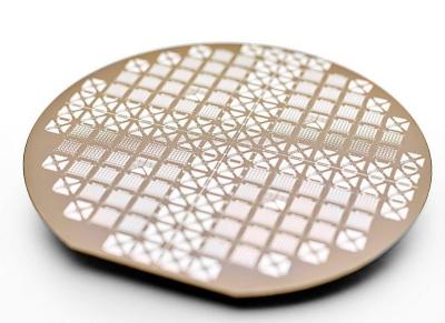
Graphenea states that in view of the market demands, the offer now includes small batch sizes (1-3 wafers). Lithography masks can be manufactured by Graphenea or provided by the customer. GFAB includes graphene growth, transfer on 4 and 6 wafers, metal contact deposition and lift-off, and graphene lithography with etching.
The devices pass the stringent quality control that Graphenea enforces on all samples, including Raman spectroscopy, optical microscopy, and electrical tests. This graphene foundry service, a first on the market, is a decisive step towards commercialization and proliferation of graphene.
GFAB is another addition to the graphene film value chain that the company offers, which has until now included graphene as-grown on copper, prepped for transfer (with PMMA coating), transferred to standard or custom substrates, and patterned into GFETs for use in sensors.