Researchers from Oxford University has found a new way of growing defect-free graphene using CVD. Defects weaken the material and prevent electronics from flowing freely through it, and this method could pave the way toward large-scale graphene production.
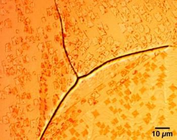
 Graphene domains across grain boundaries
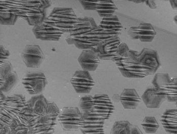
The researchers say that the random graphene flakes which are formed during the CVD process can be lined up by manipulating the alignment of carbon atoms on a relatively cheap copper foil. In fact the atomic structure of the copper surface acts as a 'guide' that controls the orientation of the carbon atoms growing on top of them. By combining the control of the copper foil and the pressure applied during growth makes it possible to control the thickness of these domains, the geometry of their edges and the grain boundaries where they meet.
 Well-aligned hexagonal graphene domains
Interestingly, just a few weeks ago we reported on research performed at the Beckman Institute that studied the electronics behavior of graphene with grain boundaries. It's good to know that we're already finding ways to control these grain boundaries.

