Grain boundaries

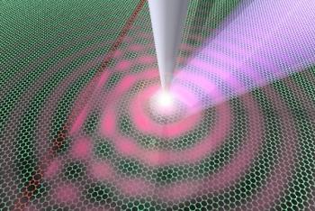
Graphene enables the ideal chemical sensor

Researchers from the University of Illinois at Chicago (UIC) developed a graphene-based highly sensitive chemical sensor (an electronic "nose" if you will). The graphene enabled the researchers to increase the sensitivity to absorbed gas molecules by 300 times compared to current technology.

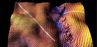
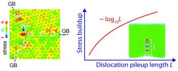
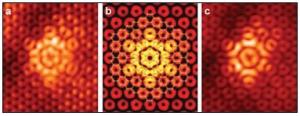
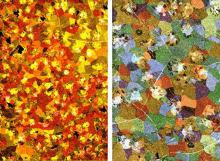
Interestingly, the graphene's grain boundaries are key to this achievement. The researchers discovered that the gas molecules are attracted to these grain boundaries, and so this is the ideal spot for the detection of these molecules. They explain that the irregular nature of the grain boundary produces hundreds of electron-transport gaps with different sensitivities - as if there are multiple switches all working in parallel.

Read the full story Posted: Sep 23,2014

Researchers find way to fix graphene grain-boundary defects

Researchers from Korea's Ulsan National Institute of Science and Technology developed a technique to repair graphene line defects by selectively depositing metal (Platinum). Graphene grain boundary defects harm the material's properties, and the new method can be used to address this issue.

Using Atomic Layer Deposition (ALD), the researchers managed to use the platinum metal and deposit it on the line defects. The researchers used the new improved sheets to develop electrodes and hydrogen gas sensors at room temperature. In these two applications, the enhanced sheets outperformed the original graphene sheets three times over.

The researchers now say they want to try different metals (such as gold and silver), and also test other applications.

Read the full story Posted: Sep 12,2014

Researchers use surface plasmons to see and study graphene grain boundaries

Researchers from the US, Germany, Singapore and Spain developed a new way to image and study grain boundary defects in graphene using surface plasmons. The idea is that by analyzing how the surface plasmons are reflected and scattered you can understand more about those defects. The researchers discovered that grain boundaries act as electronic barriers around 1020 nm in size and they are responsible for the CVD-grown graphene's low electron mobility.

In addition, the researchers say that the grain boundaries may actually be useful in the future - perhaps used as tuneable plasmons reflectors and phase retarders in "plasmonic circuits".

Read the full story Posted: Oct 18,2013

Experiments prove that graphene Boundaries do not weaken the graphene sheet

Researchers from Columbia demonstrated that a graphene sheet that is stitched together from many small crystalline grains is almost as strong as perfect graphene (this depends on the processing method, though). This solves the question whether graphene defects harm its mechanical strength (some theoretical simulations predict that grain boundaries are strong while other indicated they weaken the graphene sheet).

Commonly used methods for post-processing CVD-grown graphene may indeed weaken the grain boundaries and create a low-strength graphene. But the researchers developed a new transfer process (using a different etchant) that prevents any damage to the graphene.

Read the full story Posted: Jun 02,2013

Graphene defects can make it weak as the material exhibits a Pseudo Hall-Petch effect

Researchers from Rice University and Tsinghua University discovered (using theoretical calculations) that defects in graphene can cause it to become weak - if they occur at the grain boundaries of graphene sheets. Those grain boundaries occur because graphene grown in labs (usually using CVD) are not perfect and this creates several "islands" of graphene that merge together. The researchers say that at these points, graphene is about half as strong as perfect graphene.

The atoms on the lines that connect those islands are called grain boundaries - and the atoms at those lines usually bond in five- and seven- atom rings. These are weaker than the normal hexagon rings of graphene. The weakest points are seven-atom rings. These are found at junctions of three islands, and that's where cracks in graphene are most likely to form.

Read the full story Posted: Mar 31,2013

Oxford researchers find a way to grow defect-free graphene using CVD

Researchers from Oxford University has found a new way of growing defect-free graphene using CVD. Defects weaken the material and prevent electronics from flowing freely through it, and this method could pave the way toward large-scale graphene production.

Graphene domains across grain boundariesGraphene domains across grain boundaries

The researchers say that the random graphene flakes which are formed during the CVD process can be lined up by manipulating the alignment of carbon atoms on a relatively cheap copper foil. In fact the atomic structure of the copper surface acts as a 'guide' that controls the orientation of the carbon atoms growing on top of them. By combining the control of the copper foil and the pressure applied during growth makes it possible to control the thickness of these domains, the geometry of their edges and the grain boundaries where they meet.

Read the full story Posted: Feb 03,2013

New research into graphene grain boundaries

Researchers from the Beckman Institute have researchers the electronics behavior of graphene with grain boundaries. They explain that when graphene is grown, lattices of the carbon grains are formed randomly, linked together at different angles of orientation in a hexagonal network. But sometimes when the process is not perfect, defects called grain boundaries (GBs) form. These boundaries scatter the flow of electrons in graphene, which harms the material's electronic performance.

The researchers grew polycrystalline graphene on a silicon wafer using CVD, and then examined the atomic-scale grain boundaries using scanning tunneling microscopy and spectroscopy. The electron scattering at the boundaries significantly limits the electronic performance compared to grain boundary free graphene.  In fact they say that when the electrons' itinerary takes them to a grain boundary, it is like hitting a hill - the electrons bounce off, interfere with themselves and create a wave pattern. The hill slows the electrons down - which means that the grain boundary is a resistor in series with a conductor.

Read the full story Posted: Jan 16,2013

Defects in Graphene can make it even stronger

NIST researchers say that defects in Graphene may appear due to the movement of the carbon atoms at high temperatures when producing graphene by heating silicon carbide under ultrahigh vacuum. Graphene tend to rearrange from six-sided rings to five or seven atoms. Stringing five and seven member rings together in closed loops creates a new type of defect or grain boundary loop in the honeycomb lattice. These defects might allow it a little flexibility, making Graphene even more resilient to tearing or fracturing.

The researchers say that we should be able to either avoid defects entirely or produce them at will by variations in growth conditions.

Read the full story Posted: May 25,2011

Researchers study graphene grain boundaries and create beautiful images

Researchers from Cornell are studying Graphene grain boundaries. The researchers say that graphene doesn't grow in perfect sheets - it rather develops in pieces that resemble patchwork quilts. The meeting point of those patches is called grain boundaries, and the researchers are studying those boundaries.

The researchers grew Graphene on copper and then conceived a novel way to peel them off as free-standing, atom-thick films. They imaged the graphene (using diffraction imaging electron microscopy) and used a color to represent the angle that electrons bounced off at. Using different colors based on the electron bounce they created an easy way to image graphene grain boundaries. This method could also be applied to other 2D materials - and help explain the way that Graphene was stitched together at the boundaries.

Read the full story Posted: Jan 07,2011