Researchers from Georgia Tech have developed a new low-temperature method to dope graphene films using self-assembled monolayers (SAM) that modify the interface of graphene and its support substrate. Using this method the researchers developed graphene p-n junctions.
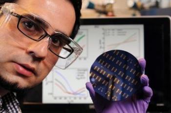
The researchers used CVD to grow graphene on copper film and then transferred it to silicon dioxide substrates that were functionalized with the self-assembled monolayers. Thus they have shown that you can make fairly well doped p-type and n-type graphene controllably by patterning the underlying monolayer instead of modifying the graphene directly. All previous methods (such as substitution of carbon atoms for nitrogen atoms, compounds addition or graphene ribbons edge modification) or had disrupted the graphene lattice which reduced the electron mobility and the devices were not stable.
The researchers are also developing new precursor materials that will enable graphene production using CVD at low temperatures - so it can be fabricated directly on other devices (instead of moving it from the original substrate to the target one). Such a low-cost, low-temp method will enable producing larger graphene sheets and will be useful in displays (LCD or OLEDs), solar panels and other applications.
Source: ScienceDaily