Researchers from the University of the Bundeswehr Munich & SENS Research Center and KTH Royal Institute of Technology recently demonstrated the noncontact and resist-free patterning of platinum diselenide (PtSe2), molybdenum disulfide (MoS2), and graphene layers with nanoscale precision at high processing speed while preserving the integrity of the surrounding material.
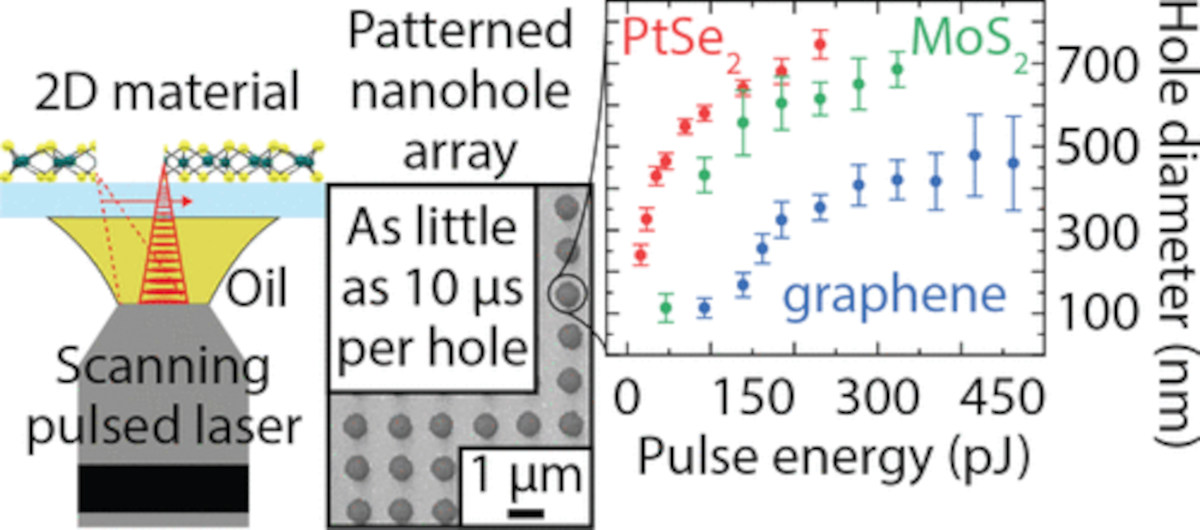
The team used a commercial, off-the-shelf two-photon 3D printer to directly write patterns in the 2D materials with features down to 100 nm at a maximum writing speed of 50 mm/s.
Traditional methods, such as optical lithography and laser interference lithography, require coating the 2D material with a protective resist mask, allowing only specific areas of the 2D material to be exposed during etching. However, the process of coating, developing, and removing the photoresist can damage the 2D material. The technique presented in this study does not require a masking layer, thereby avoiding contamination and damaging the substrate.
In this study, the team successfully removed a continuous film of 2D material from a 200 μm × 200 μm substrate area in less than 3 s. Since two-photon 3D printers are becoming increasingly available in research laboratories and industrial facilities, the scientists expect this method to enable fast prototyping of devices based on 2D materials across various research areas.
“Providing a way to work with 2D materials outside the cleanrooms lowers the bar for engaging in this exciting field of research,” says Alessandro Enrico, one of the study’s lead authors, who used to work at the Division of Micro and Nanosystems (MST) at KTH and recently transferred to the University of Pavia in Italy. “This approach has other advantages over conventional lithographic processes: the material is not damaged or contaminated by multiple steps of coating and solvent rinsing. No chemical also means a more environment-friendly approach for 2D material research and production,” adds the researcher.
The next step is to investigate the compatibility of this method with suspended 2D material membranes and replace the glass substrate with other functional ones.
This project was done within the framework of the Graphene Flagship and the Graphene Flagship Partnering Project FLAG‐ERA JTC 2019 2D‐NEMS, which is affiliated with the Sensors Work Package of the Graphene Flagship.

