Molybdenum

Researchers design a butterfly-inspired multisensory neuromorphic platform for integration of visual and chemical cues

It is a known fact that animals require the integration of cues collected from multiple sensory organs to enhance the overall perceptual experience and thereby facilitate better decision-making in most aspects of life. However, despite the importance of multisensory integration in animals, the field of artificial intelligence (AI) and neuromorphic computing has primarily focused on processing unisensory information. This lack of emphasis on multisensory integration can be attributed to the absence of a miniaturized hardware platform capable of co-locating multiple sensing modalities and enabling in-sensor and near-sensor processing. 

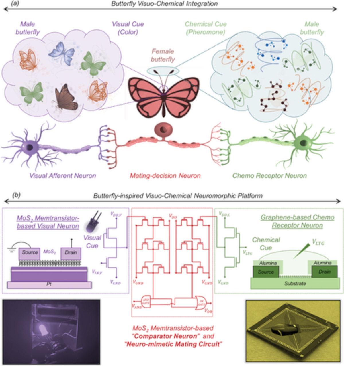
a) A simplified abstraction of visual and chemical stimuli from male butterflies and visuo-chemical integration pathway in female butterflies. b) Butterfly-inspired neuromorphic hardware comprising of monolayer MoS2 memtransistor-based visual afferent neuron, graphene-based chemoreceptor neuron, and MoS2 memtransistor-based neuro-mimetic mating circuits. Image credit: Advanced Materials

In their recent study, researchers at Penn State University addressed this limitation by utilizing the chemo-sensing properties of graphene and the photo-sensing capability of monolayer molybdenum disulfide (MoS2) to create a multisensory platform for visuochemical integration. 

Read the full story Posted: Apr 03,2024

Researchers develop unique 'Electronic tongue' using graphene and MoS2

Researchers at Penn State University recently developed an electronic “tongue” and an electronic “gustatory cortex” based on graphene ans MoS2. The artificial tastebuds comprise tiny, graphene-based electronic sensors called chemitransistors that can detect gas or chemical molecules. The other part of the circuit uses memtransistors, which is a transistor that remembers past signals, made with molybdenum disulfide. This allowed the researchers to design an “electronic gustatory cortex” that connect a physiology-drive “hunger neuron,” psychology-driven “appetite neuron” and a “feeding circuit.”   

For instance, when detecting salt, or sodium chloride, the device senses sodium ions, explained Subir Ghosh, a doctoral student in engineering science and mechanics and co-author of the study. “This means the device can ‘taste’ salt,” Ghosh said. 

Read the full story Posted: Oct 17,2023

Researchers pattern 2D materials using a commercial two-photon 3D printer

Researchers from the University of the Bundeswehr Munich & SENS Research Center and KTH Royal Institute of Technology recently demonstrated the noncontact and resist-free patterning of platinum diselenide (PtSe2), molybdenum disulfide (MoS2), and graphene layers with nanoscale precision at high processing speed while preserving the integrity of the surrounding material. 

The team used a commercial, off-the-shelf two-photon 3D printer to directly write patterns in the 2D materials with features down to 100 nm at a maximum writing speed of 50 mm/s. 

Read the full story Posted: Aug 02,2023

Researchers develop graphene/MoS2 micro-electrochemical capacitors for ultra-high charge storage

Researchers from the Indian Institute of Science have developed ultramicro-electrochemical capacitors with two-dimensional (2D) molybdenum disulphide (MoS2) and graphene-based electrodes. The development has great potential for wearables and implantable electronics as well as for sensors and miniature “smart” technology. 

The miniature energy storage device uses graphene Flakes and MoS2 alternately in each electrode - the cathode and anode. Gel was used as the electrolyte, which makes it possible to integrate micro-supercapacitors into chips. This would be difficult if not impossible with a water-soluble electrolyte. The capacitor showed a capacitance of 1.8 mF/cm2 for a single-layer structure (graphene-MoS2). The multilayer electrode structure, consisting of multiple alternating layers of graphene and molybdenum disulfide, gained 30 times greater capacitance, or 54 μF/cm2.

Read the full story Posted: Mar 16,2023

Researchers design impressive all-in-one miniature spectrometers using graphene and Mos2

An international team of researchers, including ones from Aalto University, Shanghai Jiao Tong University, Zhejiang University, Sichuan University,  Oregon State University, Yonsei University and the University of Cambridge, have designed a miniaturized spectrometer made of a ‘sandwich’ of different ingredients, including graphene, molybdenum disulfide, and tungsten diselenide. 

The spectrometer reportedly breaks all current resolution records, and does so in a much smaller package, thanks to computational programs and artificial intelligence. The new miniaturized devices could be used in a broad range of sectors, from checking the quality of food to analyzing starlight or detecting faint clues of life in outer space.

Read the full story Posted: Oct 22,2022

Researchers integrate large-area graphene-perovskite solar panels into stand-alone solar farm

An international research group, including teams from CHOSE at the University of Rome Tor Vergata, Hellenic Mediterranean University in Greece and others, has developed a large-area perovskite solar panel with graphene-doped electron transporting layers (ETLs) and functionalized molybdenum disulfide (fMoS2) buffer layers inserted between the perovskite layer and the hole transporting layer (HTL).

Nine GRAPE panels integrated in a stand-alone solar farm-powered infrastructure installed in Crete

The team reported that with increasing temperatures, the module exhibited a smaller drop in open-circuit voltage than commercially available crystalline silicon panels.

Read the full story Posted: Jun 24,2022

Researchers create miniscule graphene-MoS2 transistors

Researchers from China's Tsinghua University and East China Normal University have created a transistor with the smallest gate length ever reported. This milestone was made possible by using graphene and molybdenum disulfide and stacking them into a staircase-like structure with two steps.

Vertical MoS2 transistors with sub-1-nm gate lengths imageThe structure of the side-wall transistor: Silicon dioxide base (dark blue), aluminum covered in aluminum oxide (brown ), the thin, light blue strip is graphene, the yellow and black strip is molybdenum disulfide, and underneath it, the hafnium dioxide.

On the higher step, there is the source, and on top of the lower step, there is the drain. Both are made of a titanium palladium alloy separated by the surface of the stairs, which is made of a single sheet of a molybdenum disulfide (MoS2), itself resting on a layer of hafnium dioxide that acts as an electrical insulator.

Read the full story Posted: Mar 15,2022

Researchers experiment with LIG to create improved wearable health devices

A Penn State-led international research team (led by Professor Huanyu Larry Cheng at Penn State) recently published two studies that could boost research and development of future motion detection, tactile sensing and health monitoring devices.

Graphene made with lasers for wearable health devices image

There are various substances that can be converted into carbon to create graphene through laser radiation, in a process called laser-induced graphene (LIG). The resulting product can have specific properties determined by the original material. The team set out to test this process and has reached interesting conclusions.

Read the full story Posted: Sep 04,2021

Graphene ‘nano-origami’ could enable tiny microchips

Scientists at the University of Sussex have developed a technique for making tiny microchips from graphene and other 2D materials, using a form of ‘nano-origami’.

By creating distortions in the structure of the graphene, the researchers were able to make the nanomaterial behave like a transistor. We’re mechanically creating kinks in a layer of graphene, says Professor Alan Dalton of the School of Mathematical and Physics Sciences at the University of Sussex. It’s a bit like nano-origami. Using these nanomaterials will make our computer chips smaller and faster. It is absolutely critical that this happens as computer manufacturers are now at the limit of what they can do with traditional semiconducting technology. Ultimately, this will make our computers and phones thousands of times faster in the future.

Read the full story Posted: Feb 16,2021

New technique may enable large-area integration of 2D materials

Researchers affiliated with the Graphene Flagship from RWTH Aachen University, Universität der Bundeswehr München and AMO in Germany, KTH Royal Institute of Technology in Sweden and with Protemics have reported a new method to integrate graphene and 2D materials into semiconductor manufacturing lines, a milestone for the recently launched 2D-EPL project.

Schematic illustration of the methodology for wafer-level transfer of two-dimensional materials imageImage from Nature Communications

Two-dimensional (2D) materials have a huge potential for providing devices with much smaller size and extended functionalities with respect to what can be achieved with today's silicon technologies. But to exploit this potential, it is vital to be able to integrate 2D materials into semiconductor manufacturing lines - a notoriously difficult step. This new technique could be a step in the right direction as far as solving this problem is concerned.

Read the full story Posted: Feb 15,2021