Researchers from China's Tsinghua University and East China Normal University have created a transistor with the smallest gate length ever reported. This milestone was made possible by using graphene and molybdenum disulfide and stacking them into a staircase-like structure with two steps.
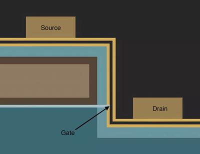
 The structure of the side-wall transistor: Silicon dioxide base (dark blue), aluminum covered in aluminum oxide (brown ), the thin, light blue strip is graphene, the yellow and black strip is molybdenum disulfide, and underneath it, the hafnium dioxide.
On the higher step, there is the source, and on top of the lower step, there is the drain. Both are made of a titanium palladium alloy separated by the surface of the stairs, which is made of a single sheet of a molybdenum disulfide (MoS2), itself resting on a layer of hafnium dioxide that acts as an electrical insulator.
The trick to this design is that the edge of the graphene sheet is used, which means that when the gate is set to the "on" state, it's only 0.34 nm wideâessentially the width of the graphene layer itself. Another notable feature of this "side-wall transistor" is its negligible current leakage due to higher off-state resistance. Manufacturers could leverage this quality for low-power applications. Best of all, it would be relatively easy to make, although many of the prototypes required quite a bit of voltage to drive.
The research team believes going smaller than 0.34 nm for the gate size is almost impossible.
The researchers behind the new transistor managed to prove that a functional transistor could be made using one-atom thin materials without inventing a new process for precision positioning of the required layers. However, reliably building billions of these side-wall transistors is still a major challenge.
In the meantime, many companies are working on making gate-all-around (GAA-FET) transistors a reality and standardizing interconnects for chiplet designs.