Researchers from Korea University have developed a simple and microelectronics-compatible method to grow graphene and have declared the successful synthesis of wafer-scale (four inches in diameter), high-quality, multi-layer graphene on silicon substrates. The method is based on an ion implantation technique, a process in which ions are accelerated under an electrical field and smashed into a semiconductor. The impacting ions change the physical, chemical or electrical properties of the semiconductor.
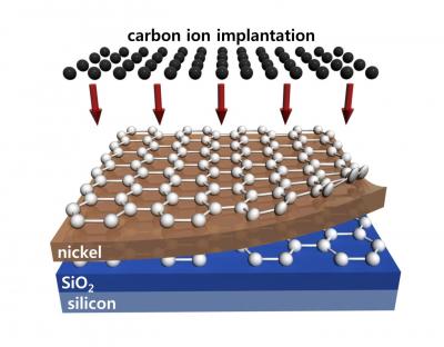
Ion implantation is a technique normally used to introduce impurities into semiconductors. In the process, carbon ions were accelerated under an electrical field and bombarded onto a layered surface made of nickel, silicon dioxide and silicon at the temperature of 500 degrees Celsius. The nickel layer, with high carbon solubility, is used as a catalyst for graphene synthesis. The process is then followed by high temperature activation annealing (about 600 to 900 degrees Celsius) to form a honeycomb lattice of carbon atoms, a typical microscopic structure of graphene.
The scientists view their method as able to take graphene a step closer to commercial applications in silicon microelectronics. The method also offers finer control on the final structure of the product than other fabrication methods, as the graphene layer's thickness can be precisely determined by controlling the dose of carbon ion implantation. The researchers' next step is to lower the temperature in the synthesis process and to control the thickness of the graphene for manufacturing production.

